MT9043 查看數據表(PDF) - Zarlink Semiconductor Inc
零件编号
产品描述 (功能)
生产厂家
MT9043 Datasheet PDF : 29 Pages
| |||
MT9043
Data Sheet
All frame pulse and clock outputs have limited driving capability, and should be buffered when driving high
capacitance (e.g., 30pF) loads.
Input Impairment Monitor
This circuit monitors the input signal to the DPLL for a complete loss of incoming signal, or a large frequency shift in
the incoming signal. If the input signal is outside the Impairment Monitor Capture Range the PLL automatically
changes from Normal Mode to Free Run Mode. See AC Electrical Characteristics - Performance for the Impairment
Monitor Capture Range. When the incoming signal returns to normal, the DPLL is returned to Normal Mode.
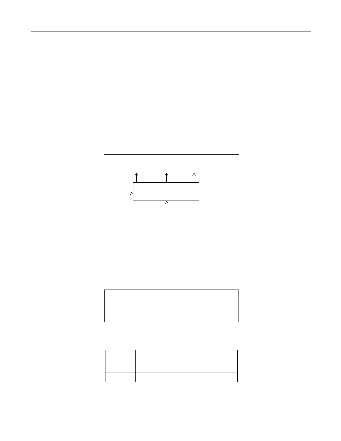
State Machine Control
As shown in Figure 1, this state machine controls the Reference Select MUX, the TIE Corrector Circuit and the
DPLL. Control is based on the logic levels at the control inputs RSEL and MS (See Figure 6).
All state machine changes occur synchronously on the rising edge of F8o. See the Control and Mode of Operation
section for full details.
To
Reference
Select MUX
To TIE
Corrector
Enable
To DPLL
State
Select
RSEL
Control
State Machine
MS
Figure 6 - Control State Machine Block Diagram
Master Clock
The MT9043 can use either a clock or crystal as the master timing source. For recommended master timing
circuits, see the Applications - Master Clock section.
Control and Mode of Operation
The active reference input (PRI or SEC) is selected by the RSEL pin as shown in Table 2.
RSEL
Input Reference
0
PRI
1
SEC
Table 2 - nput Reference Selection
MS
Mode
0
NORMAL
1
FREERUN
Table 3 - Operating Modes and States
The MT9043 has two possible modes of operation, Normal and Freerun.
8
Zarlink Semiconductor Inc.
Share Link: 