MM74HC4538 查看數據表(PDF) - Fairchild Semiconductor
零件编号
产品描述 (功能)
生产厂家
MM74HC4538 Datasheet PDF : 10 Pages
| |||
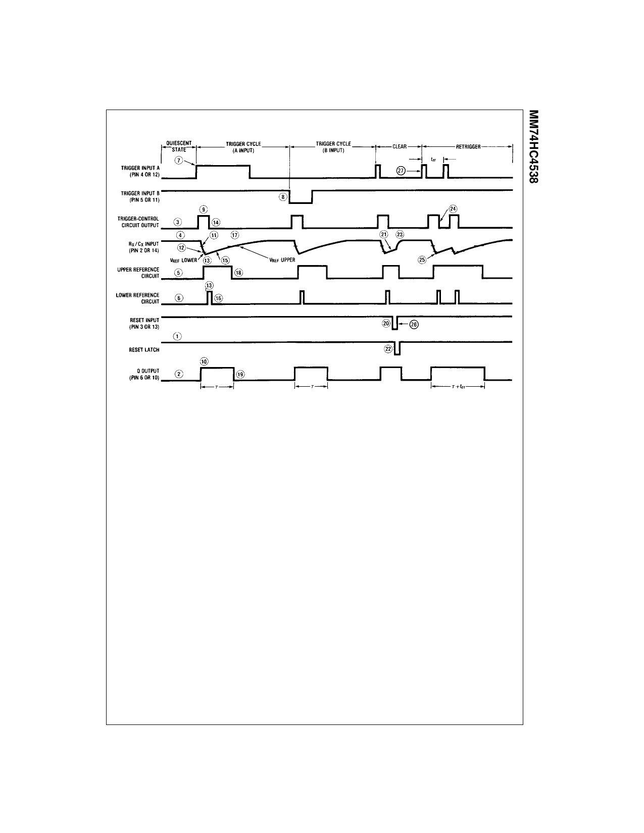
Timing Diagram
Circuit Operation
The MM74HC4538 operates as follows (refer to logic dia-
gram). In the quiescent state, the external timing capacitor,
CX, is charged to VCC. When a trigger occurs, the Q output
goes HIGH and CX discharges quickly to the lower refer-
ence voltage (VREF Lower = 1/3 VCC). CX then charges,
through RX, back up to the upper reference voltage (VREF
Upper = 2/3 VCC), at which point the one-shot has timed out
and the Q output goes LOW.
The following, more detailed description of the circuit oper-
ation refers to both the logic diagram and the timing dia-
gram.
QUIESCENT STATE
In the quiescent state, before an input trigger appears, the
output latch is HIGH and the reset latch is HIGH (#1 in logic
diagram).
Thus the Q output (pin 6 or 10) of the monostable multivi-
brator is LOW (#2, timing diagram).
The output of the trigger-control circuit is LOW (#3), and
transistors M1, M2, and M3 are turned off. The external
timing capacitor, CX, is charged to VCC (#4), and the upper
reference circuit has a LOW output (#5). Transistor M4 is
turned ON and transmission gate T1 is turned OFF. Thus
the lower reference circuit has VCC at the noninverting
input and a resulting LOW output (#6).
In addition, the output of the trigger-control reset circuit is
LOW.
TRIGGER OPERATION
The MM74HC4538 is triggered by either a rising-edge sig-
nal at input A (#7) or a falling-edge signal at input B (#8),
with the unused trigger input and the Reset input held at
the voltage levels shown in the Truth Table. Either trigger
signal will cause the output of the trigger-control circuit to
go HIGH (#9).
The trigger-control circuit going HIGH simultaneously ini-
tiates three events. First, the output latch goes LOW, thus
taking the Q output of the HC4538 to a HIGH State (#10).
Second, transistor M3 is turned on, which allows the exter-
nal timing capacitor, CX, to rapidly discharge toward
ground (#11). (Note that the voltage across CXappears at
the input of the upper reference circuit comparator.) Third,
transistor M4 is turned off and transmission gate T1 is
turned ON, thus allowing the voltage across CX to also
appear at the input of the lower reference circuit compara-
tor.
When CX discharges to the reference voltage of the lower
reference circuit (#12), the outputs of both reference cir-
cuits will be HIGH (#13). The trigger-control reset circuit
goes HIGH, resetting the trigger-control circuit flip-flop to a
LOW State (#14). This turns transistor M3 OFF again,
allowing CX to begin to charge back up toward VCC, with a
time constant t = RXCX (#15). In addition, transistor M4 is
turned ON and transmission gate T1 is turned OFF. Thus a
high voltage level is applied to the input of the lower refer-
ence circuit comparator, causing its output to go LOW
(#16). The monostable multivibrator may be retriggered at
any time after the trigger-control circuit goes LOW.
When CX charges up to the reference voltage of the upper
reference circuit (#17), the output of the upper reference
circuit goes LOW (#18). This causes the output latch to
3
www.fairchildsemi.com
Share Link: 