MC74HC73D 查看數據表(PDF) - Motorola => Freescale
零件编号
产品描述 (功能)
生产厂家
MC74HC73D Datasheet PDF : 5 Pages
| |||
MOTOROLA
SEMICONDUCTOR TECHNICAL DATA
Dual J-K Flip-Flop with Reset
High–Performance Silicon–Gate CMOS
The MC74HC73 is identical in pinout to the LS73. The device inputs are
compatible with standard CMOS outputs; with pullup resistors, they are
compatible with LSTTL outputs.
Each flip flop is negative–edge clocked and has an active–low asynchro-
nous reset.
The MC74HC73 is identical in function to the HC107, but has a different
pinout.
• Output Drive Capability: 10 LSTTL Loads
• Outputs Directly Interface to CMOS, NMOS, and TTL
• Operating Voltage Range: 2 to 6 V
• Low Input Current: 1 µA
• High Noise Immunity Characteristic of CMOS Devices
• In Compliance with the Requirements Defined by JEDEC Standard
No. 7A
• Chip Complexity: 92 FETs or 23 Equivalent Gates
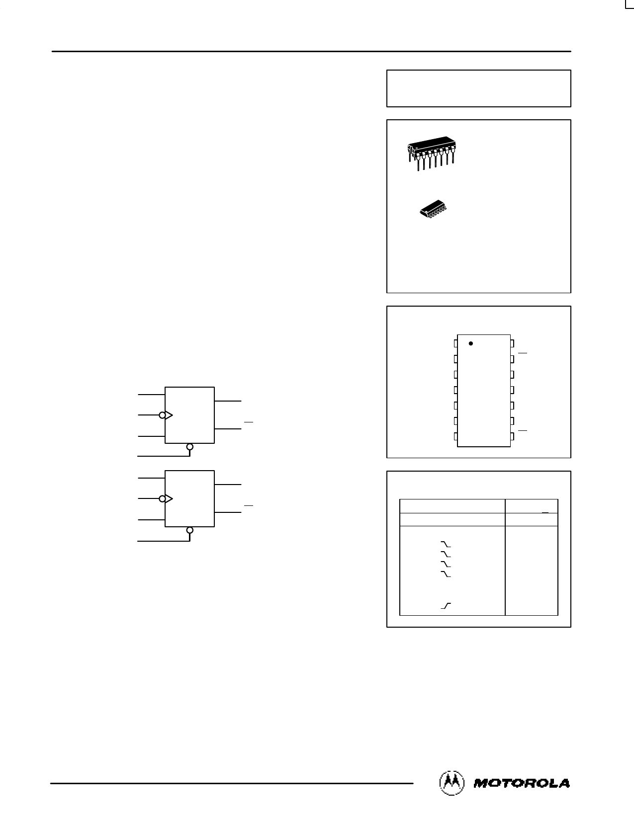
LOGIC DIAGRAM
J1
CLOCK 1
K1
RESET 1
J2
CLOCK 2
K2
RESET 2
14
1
3
2
7
5
10
6
PIN 4 = VCC
PIN 11 = GND
12
Q1
13
Q1
9
Q2
8
Q2
MC74HC73
14
1
14
1
N SUFFIX
PLASTIC PACKAGE
CASE 646–06
D SUFFIX
SOIC PACKAGE
CASE 751A–03
ORDERING INFORMATION
MC74HCXXN
MC74HCXXD
Plastic
SOIC
PIN ASSIGNMENT
CLOCK 1 1
RESET 1 2
K1 3
VCC 4
CLOCK 2 5
RESET 2 6
J2 7
14 J1
13 Q1
12 Q1
11 GND
10 K2
9 Q2
8 Q2
FUNCTION TABLE
Inputs
Reset Clock J
L
XX
H
L
H
L
H
H
H
H
H
LX
H
HX
H
X
Outputs
KQQ
XLH
L No Change
HLH
LHL
H
Toggle
X No Change
X No Change
X No Change
10/95
© Motorola, Inc. 1995
1
REV 6
Share Link: 