MC10H600 查看數據表(PDF) - ON Semiconductor
零件编号
产品描述 (功能)
生产厂家
MC10H600 Datasheet PDF : 6 Pages
| |||
MC10H600, MC100H600
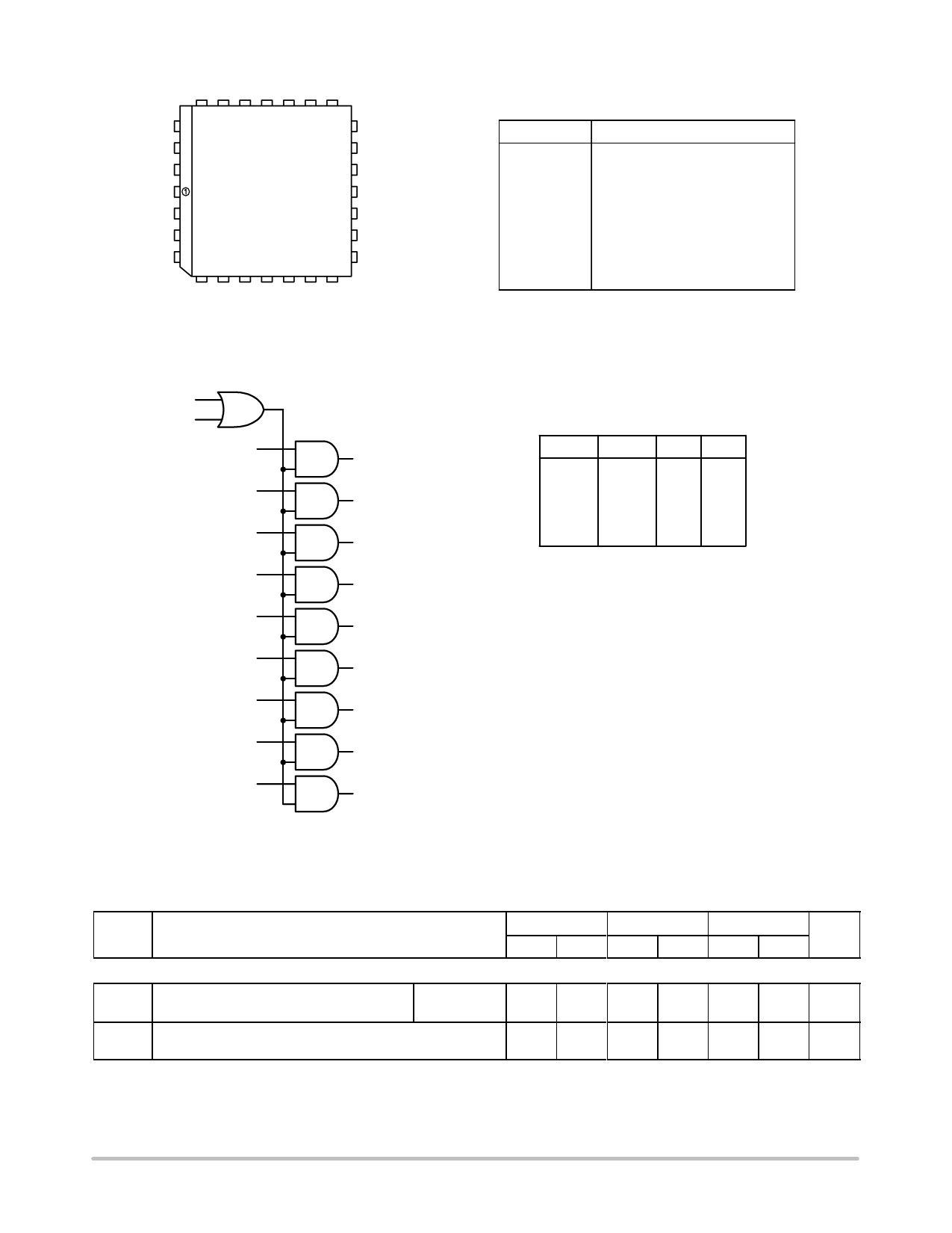
D5 D4 VCCT D3 D2 D1 D0
25 24 23 22 21 20 19
D6 26
18 Q0
D7 27
17 Q1
D8 28
GND
ENTTL 2
16 VCCE
15 VCCO
14 Q2
NC 3
13 VCCO
ENECL 4
12 Q3
5 6 7 8 9 10 11
Q8 Q7 VCCO Q6 VEE Q5 Q4
Figure 1. Pinout: PLCC−28 (Top View)
Table 1. PIN NAMES
PIN
FUNCTION
GND
VCCE
VCCO
VCCT
VEE
D0 −D8
Q0 −Q8
ENECL
ENTTL
TTL Ground (0 V)
ECL VCC (0 V)
ECL VCC (0 V) − Outputs
TTL Supply (+ 5.0 V)
ECL Supply (− 5.2 / −4.5 V)
Data Inputs (TTL)
Data Outputs (ECL)
Enable Control (ECL)
Enable Control (TTL)
ENECL
ENTTL
D0
D1
D2
D3
TTL D4
D5
D6
D7
D8
Q0
Q1
Q2
Q3
ECL
Q4
Q5
Q6
Q7
Q8
Figure 2. Logic Symbol
Table 2. TRUTH TABLE
ENECL ENTTL D
Q
H
X
H
H
H
X
L
L
X
H
H
H
X
H
L
L
L
L
X
L
Table 3. DC CHARACTERISTICS: VCCT = 5.0 V ± 10%; VEE = − 5.2 V ± 5% (10H version); VEE = − 4.2 V to − 5.5 V (100H)
0°C
25°C
75°C
Symbol
Power Supply Current
Parameter
Min Max Min Max Min Max Unit
IEE
ECL
10H
100H
−125
−122
−125
−123
−125 mA
−132
ICCH
TTL
ICCL
48
48
48
mA
50
50
50
NOTE: Device will meet the specifications after thermal equilibrium has been established when mounted in a test socket or printed circuit
board with maintained transverse airflow greater than 500 lfpm. Electrical parameters are guaranteed only over the declared
operating temperature range. Functional operation of the device exceeding these conditions is not implied. Device specification limit
values are applied individually under normal operating conditions and not valid simultaneously.
http://onsemi.com
2
Share Link: 