M67204H_ 查看數據表(PDF) - Atmel Corporation
零件编号
产品描述 (功能)
生产厂家
M67204H_ Datasheet PDF : 4 Pages
| |||
Workaround
The workaround depends of the available means to implement it. Any of the following workarounds can be used:
1. No read sequence while write sequence.
2. Control the distance between the read and write locations.
3. Control the tWLRL parameter in accordance with the above table.
4. Apply a read pulse tRLRH greater than the value given in the above table.
2. Empty Flag Parasitic Pulse.
Description
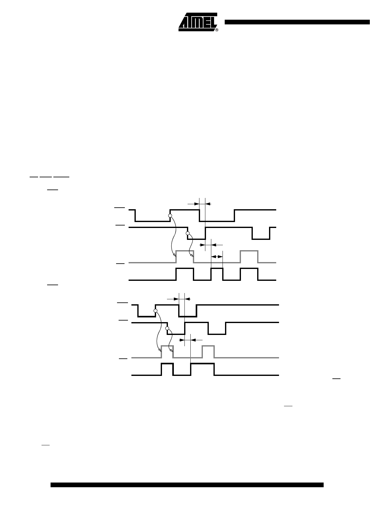
A parasitic positive pulse can be obseved during a FIFO write if it is applied during the read of first data of the FIFO
buffer (c.f. hereunder chronograms).
Side Effect
No side effect on flags computation, internal FIFO control and data integrity.
Behavior
1. WR wide pulse width:
WR
Data0
tWLRH
RD
Expected
EF
Observed
tRHEH
tpulse
2. WR short pulse width:
tWLRH
WR Data0
RD
Expected
EF
Observed
tRHEH
In this case, the falling edge of the parasitic pulse is masked by the beginning of the regular hight level of EF flag.
Root Cause
Un-controlled delays on input signals of a flags logic decoder generate an internal glitch. This glitch is re-formatted by
the on-chip ETD system (Edge Transition Detection) and a parasitic pulse is output on EF pin.
Work Around
Any of the following workarounds can be used:
1. No write sequence while read sequence.
2. EF evaluation according to the following characterization.
2
4425B–AERO–01/06
Share Link: 