LTC5530ES6 查看數據表(PDF) - Linear Technology
零件编号
产品描述 (功能)
生产厂家
LTC5530ES6 Datasheet PDF : 12 Pages
| |||
LTC5530
APPLICATIO S I FOR ATIO
Operation
The LTC5530 RF detector integrates several functions to
provide RF power detection over frequencies ranging from
300MHz to 7GHz. These functions include an internal fre-
quency compensated buffer amplifier, an RF Schottky di-
ode peak detector and level shift amplifier to convert the RF
input signal to DC and a delay circuit to avoid voltage tran-
sients at VOUT when powering up. The LTC5530 has both
shutdown and gain setting capabilities.
Buffer Amplifier
The output buffer amplifier is capable of supplying typi-
cally 4mA into a load. The negative terminal VM is brought
out to a pin for gain selection. External resistors connected
between VOUT and VM (RA) and VM to ground (RB) will set
the amplifier gain.
GAIN = 1+ RA
RB
The amplifier is unity gain stable; however a minimum gain
of two is recommended to improve low output voltage
accuracy. The amplifier bandwidth is 2MHz for a gain of 2.
For increased gain applications, the bandwidth is reduced
according to the formula:
BANDWIDTH = 4MHz = 4MHz • RB
(GAIN)
(RA + RB)
A capacitor can be placed across the feedback resistor RA
to shape the frequency response. In addition the amplifier
can be used as a comparator. VM can be connected to a
reference voltage. When the internal detector voltage
(which is connected to the positive input of the buffer
amplifier) exceeds the external voltage of VM, VOUT will
switch high.
RF Detector
The internal RF Schottky diode peak detector and level
shift amplifier converts the RF input signal to a low
frequency signal. The detector demonstrates excellent
efficiency and linearity over a wide range of input power.
The Schottky diode is biased at about 55µA and drives a
25pF internal peak detector capacitor.
Shutdown
The part is in shutdown mode when SHDN is low. The
supply current is reduced to < 2µA and VOUT is shorted to
ground via a 280Ω resistor. When SHDN is asserted high,
the part is enabled after about 8µs.
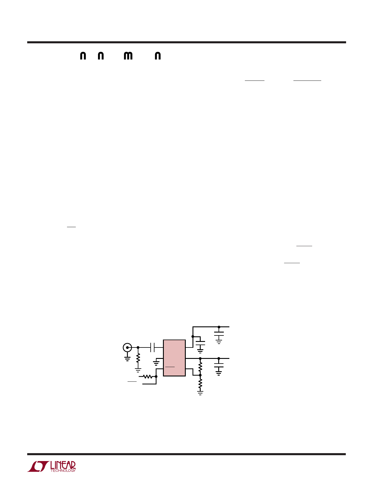
Demo Board Schematic
C4 LTC5530ES6
RFIN
39pF
1
6
RFIN VCC
R1
(OPT)
R2
22k
VCC
2
5
GND VOUT
3
4
SHDN VM
SHDN
C2
100pF
VCC
2.7V TO 6V
C1
0.1µF
VOUT
R3
C3
10k
(OPT)
R4
10k
5530 DB
5530f
9
Share Link: 