IW4027B 查看數據表(PDF) - Integral Corp.
零件编号
产品描述 (功能)
生产厂家
IW4027B Datasheet PDF : 6 Pages
| |||
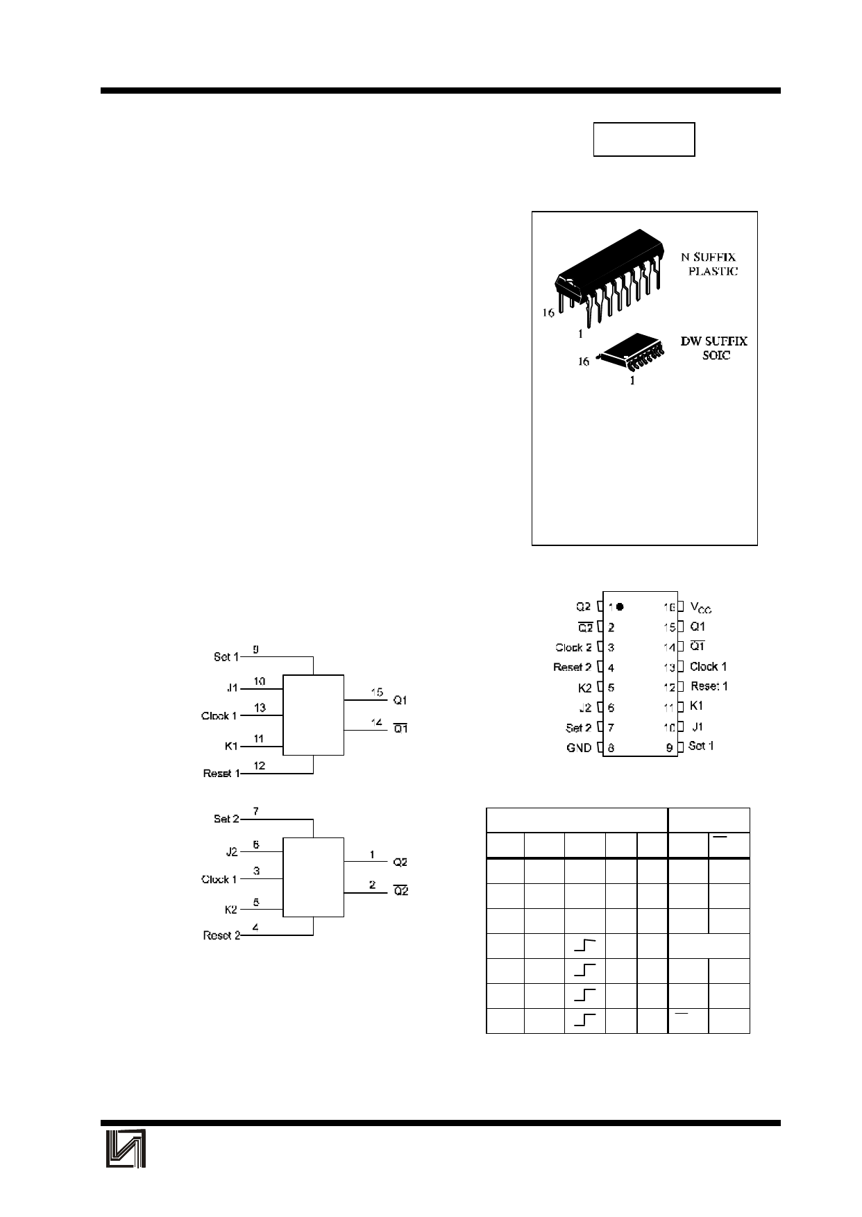
TECHNICAL DATA
Dual JK Flip-Flop
IW4027B
The IW4027B is a Dual JK Flip-Flop which is edge-triggered and
features independent Set, Reset, and Clock inputs. Data is accepted
when the Clock is LOW and transferred to the output on the positive-
going edge of the Clock. The active HIGH asynchronous Reset and Set
are independent and override the J, K, or Clock inputs. The outputs are
buffered for best system performance.
• Operating Voltage Range: 3.0 to 18 V
• Maximum input current of 1 µA at 18 V over full package-
temperature range; 100 nA at 18 V and 25°C
• Noise margin (over full package temperature range):
1.0 V min @ 5.0 V supply
2.0 V min @ 10.0 V supply
2.5 V min @ 15.0 V supply
ORDERING INFORMATION
IW4027BN Plastic
IW4027BD SOIC
IZ4027B Chip
TA = -55° to 125° C for all packages
LOGIC DIAGRAM
PIN ASSIGNMENT
PIN 16 =VCC
PIN 8 = GND
INTEGRAL
FUNCTION TABLE
Inputs
Outputs
Set Reset Clock J K Qn+1 Qn+1
L H X XX L H
H L X XX H L
H H X XX H H
LL
L L No change
LL
HL H L
LL
LH L H
LL
H H Qn Qn
X = don’t care
Qn+1 = State After Clock Positive Transition
1
Share Link: 