IDT72205LB10J8(2017) 查看數據表(PDF) - Integrated Device Technology
零件编号
产品描述 (功能)
生产厂家
IDT72205LB10J8
(Rev.:2017)
(Rev.:2017)
Integrated Device Technology
IDT72205LB10J8 Datasheet PDF : 16 Pages
| |||
CMOS SyncFIFOTM
256 x 18, 512 x 18, 1,024 x 18,
2,048 x 18, and 4,096 x 18
IDT72205LB, IDT72215LB,
IDT72225LB, IDT72235LB,
IDT72245LB
LEAD FINISH (SnPb) ARE IN EOL PROCESS - LAST TIME BUY EXPIRES JUNE 15, 2018
FEATURES:
• 256 x 18-bit organization array (IDT72205LB)
• 512 x 18-bit organization array (IDT72215LB)
• 1,024 x 18-bit organization array (IDT72225LB)
• 2,048 x 18-bit organization array (IDT72235LB)
• 4,096 x 18-bit organization array (IDT72245LB)
• 10 ns read/write cycle time
• Empy and Full flags signal FIFO status
• Easy expandable in depth and width
• Asynchronous or coincident read and write clocks
• Programmable Almost-Empty and Almost-Full flags with
default settings
• Half-Full flag capability
• Dual-Port zero fall-through time architecture
• Output enable puts output data bus in high-impedence state
• High-performance submicron CMOS technology
• Available in a 64-lead thin quad flatpack (TQFP/STQFP)
and plastic leaded chip carrier (PLCC)
• Industrial temperature range (–40°C to +85°C) is available
• Green parts available, see ordering information
DESCRIPTION:
The IDT72205LB/72215LB/72225LB/72235LB/72245LB are very high
speed, low-power First-In, First-Out (FIFO) memories with clocked read and
write controls. These FIFOs are applicable for a wide variety of data buffering
needs, such as optical disk controllers, Local Area Networks (LANs), and
interprocessor communication.
These FIFOs have 18-bit input and output ports. The input port is controlled
by a free-running clock (WCLK), and an input enable pin (WEN). Data is read
into the synchronous FIFO on every clock when WEN is asserted. The output
port is controlled by another clock pin (RCLK) and another enable pin (REN).
The read clock can be tied to the write clock for single clock operation or the
two clocks can run asynchronous of one another for dual-clock operation. An
Output Enable pin (OE) is provided on the read port for three-state control of
the output.
The synchronous FIFOs have two fixed flags, Empty (EF) and Full (FF),
and two programmable flags, Almost-Empty (PAE) and Almost-Full (PAF). The
offset loading of the programmable flags is controlled by a simple state machine,
and is initiated by asserting the Load pin (LD). A Half-Full flag (HF) is available
when the FIFO is used in a single device configuration.
These devices are depth expandable using a Daisy-Chain technique. The
XI and XO pins are used to expand the FIFOs. In depth expansion configu-
ration, First Load (FL) is grounded on the first device and set to HIGH for all
other devices in the Daisy Chain.
The IDT72205LB/72215LB/72225LB/72235LB/72245LB is fabricated
using high-speed submicron CMOS technology.
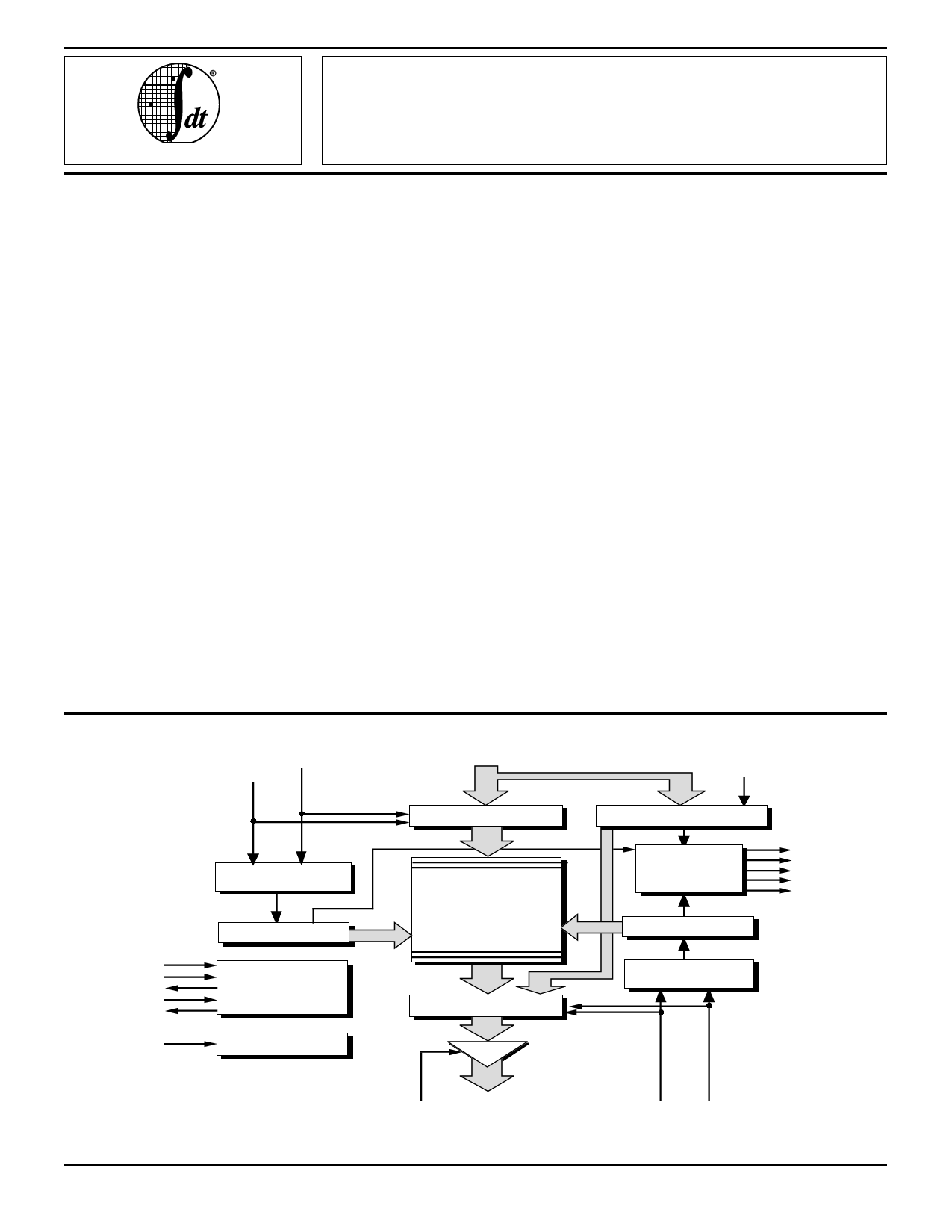
FUNCTIONAL BLOCK DIAGRAM
WCLK
D0-D17
( )/
WRITE CONTROL
LOGIC
WRITE POINTER
EXPANSION LOGIC
RESET LOGIC
INPUT REGISTER
••
RAM ARRAY
256 x 18, 512 x 18
1,024 x 18, 2,048 x 18
4,096 x 18
••
OUTPUT REGISTER
OFFSET REGISTER
FLAG
LOGIC
READ POINTER
READ CONTROL
LOGIC
/( )
Q0-Q17
RCLK
IDT and the IDT logo are registered trademarks of Integrated Device Technology, Inc. SyncFIFO is a trademark of Integrated Device Technology, Inc.
COMMERCIAL AND INDUSTRIAL TEMPERATURE RANGES
1
©2017 Integrated Device Technology, Inc. All rights reserved. Product specifications subject to change without notice.
2766 drw 01
NOVEMBER 2017
DSC-2766/4
Share Link: 