FOD8320 查看數據表(PDF) - Fairchild Semiconductor
零件编号
产品描述 (功能)
生产厂家
FOD8320
Fairchild Semiconductor
FOD8320 Datasheet PDF : 19 Pages
| |||
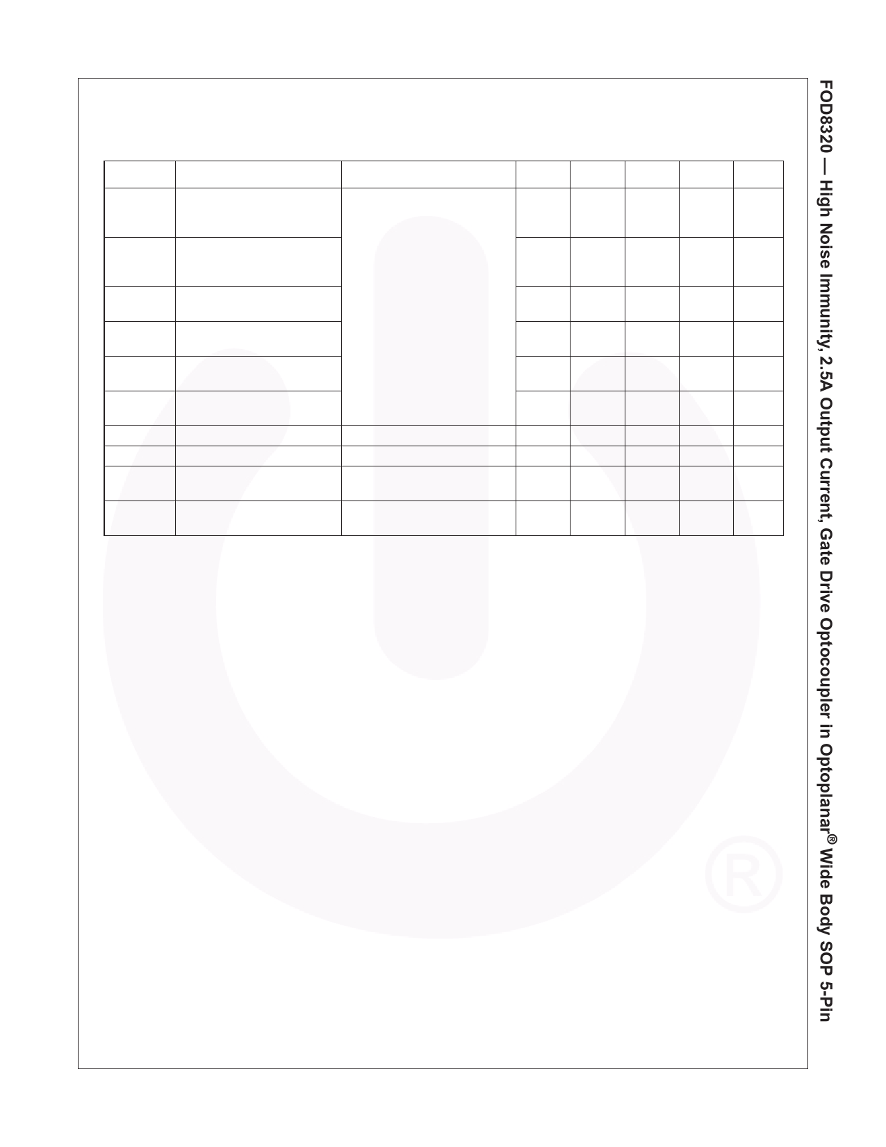
Switching Characteristics
Apply over all recommended conditions, typical value is measured at VDD = 30V, VSS = Ground, TA = 25°C unless
otherwise specified.
Symbol
Parameter
Conditions
Min. Typ. Max. Units Figure
tPHL
Propagation Delay Time to
IF = 7mA to 16mA, Rg = 10Ω,
150
285
400
Logic Low Output(9)
Cg =10nF, f = 10kHz,
Duty Cycle = 50%
ns 10, 11,
12, 13,
14, 27
tPLH
Propagation Delay Time to
Logic High Output(10)
PWD
PDD
(Skew)
Pulse Width Distortion(11)
|tPHL – tPLH|
Propagation Delay Difference
Between Any Two Parts(12)
150
260
400
25
100
-250
250
ns 10, 11,
12, 13,
14, 27
ns
tR
Output Rise Time
(10% to 90%)
60
ns
27
tF
Output Fall Time
(90% to 10%)
60
ns
27
tULVO ON ULVO Turn On Delay
IF = 10mA, VO > 5V
0.8
tULVO OFF ULVO Turn Off Delay
IF = 10mA, VO < 5V
0.4
|CMH| Common Mode Transient
TA = 25°C, VDD = 30V,
35
50
Immunity at Output High
IF = 7 to 16mA, VCM = 2000V(13)
|CML| Common Mode Transient
TA = 25°C, VDD = 30V, VF = 0V,
35
50
Immunity at Output Low
VCM = 2000V(14)
µs
µs
kV/µs
28
kV/µs
28
Notes:
9. tPHL propagation delay is measured from the 50% level on the falling edge of the input pulse to the 50% level of the
falling edge of the VO signal.
10. tPLH propagation delay is measured from the 50% level on the rising edge of the input pulse to the 50% level of the
rising edge of the VO signal.
11. PWD is defined as | tPHL – tPLH | for any given device.
12. The difference between tPHL and tPLH between any two FOD8320 parts under same operating conditions, with equal
loads.
13. Common mode transient immunity at output high is the maximum tolerable negative dVcm/dt on the trailing edge of
the common mode impulse signal, Vcm, to assure that the output will remain high (i.e. VO > 15.0V).
14. Common mode transient immunity at output low is the maximum tolerable positive dVcm/dt on the leading edge of
the common pulse signal, Vcm, to assure that the output will remain low (i.e. VO < 1.0V).
©2010 Fairchild Semiconductor Corporation
FOD8320 Rev. 1.0.6
6
www.fairchildsemi.com
Share Link: 