DS1135LZ 查看數據表(PDF) - Dallas Semiconductor -> Maxim Integrated
零件编号
产品描述 (功能)
生产厂家
DS1135LZ Datasheet PDF : 6 Pages
| |||
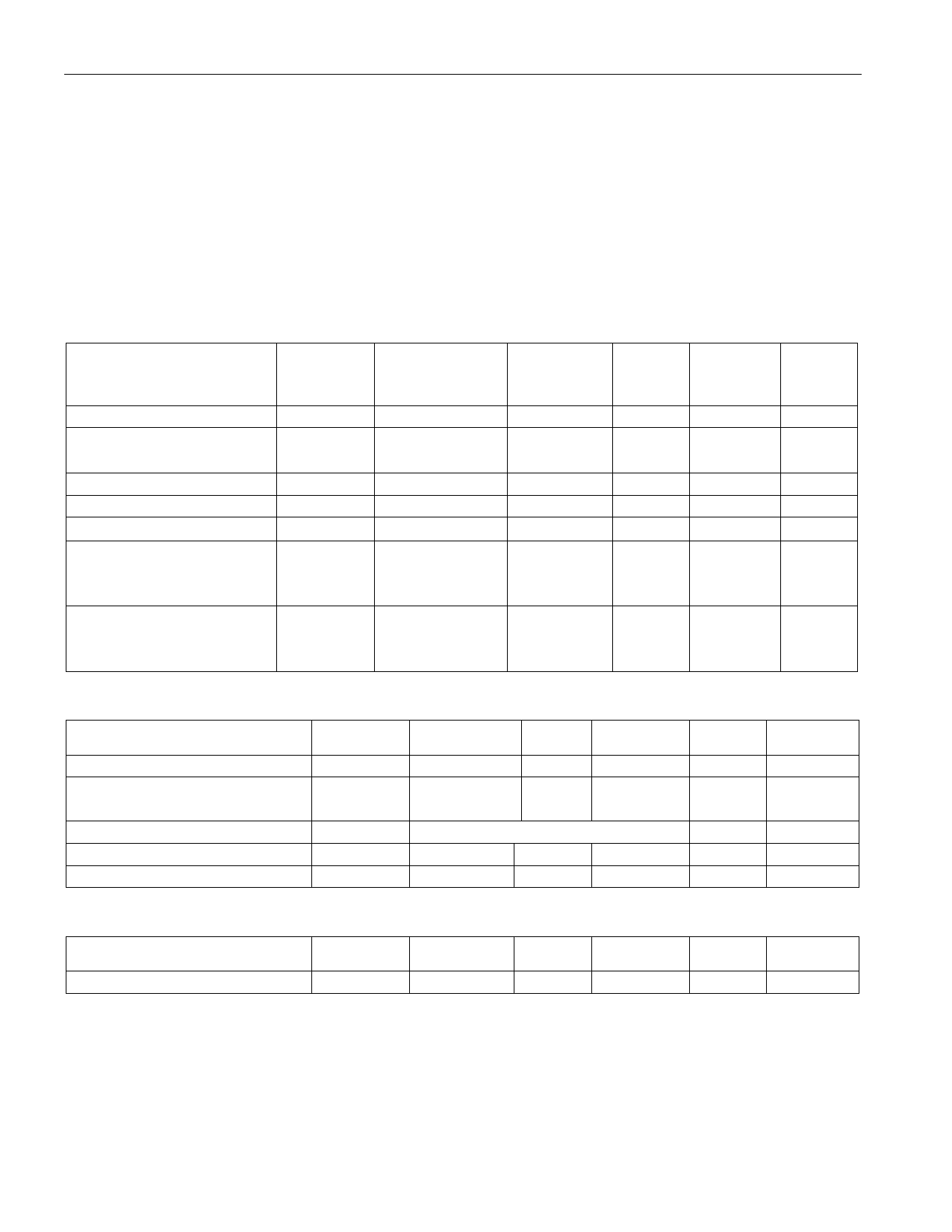
ABSOLUTE MAXIMUM RATINGS*
Voltage on Any Pin Relative to Ground
Operating Temperature
Storage Temperature
Soldering Temperature
Short Circuit Output Current
-1.0V to +6.0 V
-40°C to +85°C
-55°C to +125°C
See J-STD-020A specification
50mA for 1 second
DS1135-L
* This is a stress rating only and functional operation of the device at these or any other conditions above
those indicated in the operation sections of this specification is not implied. Exposure to absolute
maximum rating conditions for extended periods of time may affect reliability.
DC ELECTRICAL CHARACTERISTICS
PARAMETER
Supply Voltage
Active Current
High Level Input Voltage
Low Level Input Voltage
Input Leakage
High Level Output
Current
SYMBOL
VCC
ICC
VIH
VIL
IL
ICC
TEST
CONDITION
VCC =3.6V
Period=1ms
0V≤VI ≤VCC
VCC =2.7V
VOH =2V
Low Level Output
Current
ICC
VCC =2.7V
VOL=0.4V
(-40°C to +85°C;VCC=2.7-3.6V)
MIN
TYP MAX UNITS
2.7
3.3
3.6
V
10
mA
2.0
VCC +0.5
V
-0.5
0.8
V
-1.0
+1.0
mA
-1.0
mA
8
mA
AC ELECTRICAL CHARACTERISTICS
(-40°C to +85°C;VCC=2.7-3.6V)
PARAMETER
SYMBOL MIN
TYP MAX UNITS NOTES
Period
tPERIOD
2 (tWI )
ns
Input Pulse Width
tWI
100% of
Delay Value
ns
Input-to-Output Delay
tPLH, tPHL
See Table 1
ns
Output Rise or Fall Time
tOF, tOR
2.0
2.5
ns
Power-up Time
tPU
1
ms
2
CAPACITANCE
PARAMETER
Input Capacitance
SYMBOL
CIN
MIN
(TA=25°C)
TYP MAX UNITS NOTES
10
pF
4 of 6
Share Link: 