DM74S175 查看數據表(PDF) - Fairchild Semiconductor
零件编号
产品描述 (功能)
生产厂家
DM74S175 Datasheet PDF : 5 Pages
| |||
Function Table (Each Flip-Flop)
Inputs
Clear
Clock
D
L
X
X
H
↑
H
H
↑
L
H
L
X
H = HIGH Level (steady state)
L = LOW Level (steady state)
X = Don’t Care
↑ = Transition from LOW-to-HIGH level
Q0 = The level of Q before the indicated steady-state input conditions were established.
Note 1: DM74S175 only.
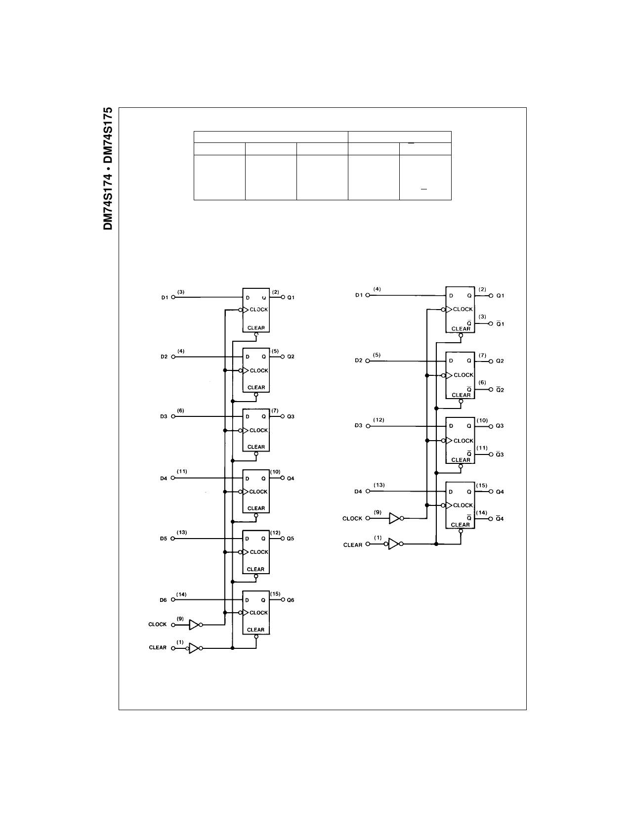
Logic Diagrams
DM74S174
Outputs
Q
Q (Note 1)
L
H
H
L
L
H
Q0
Q0
DM74S175
www.fairchildsemi.com
2
Share Link: 