ADL5303 查看數據表(PDF) - Analog Devices
零件编号
产品描述 (功能)
生产厂家
ADL5303 Datasheet PDF : 24 Pages
| |||
Data Sheet
ADL5303
APPLICATIONS INFORMATION
Smaller input voltages can be measured accurately when
aided by a small offset nulling voltage applied to VSUM.
The minimum voltage that can be accurately measured is
limited only by the drift in the input offset of the ADL5303.
The specifications show the maximum spread over the full
temperature and supply range. Over a limited temperature
range and with a regulated supply, the offset drift is lower;
in this situation, processing of inputs down to 5 mV is
practicable.
RESCALING
The use of a much larger value for the intercept may be useful
in certain situations. In this example, it has been moved up four
decades, from the default value of 100 pA to the center of the
full eight-decade range at 1 mA. Using a voltage input as previ-
ously described, this corresponds to an altered voltage mode
intercept, VZ, which is 1 V for RIN = 1 MΩ. To take full advantage
of the larger output swing, the gain of the buffer has been
increased to 4.53, resulting in a scaling of 900 mV/decade
zand a full-scale output of ±3.6 V.
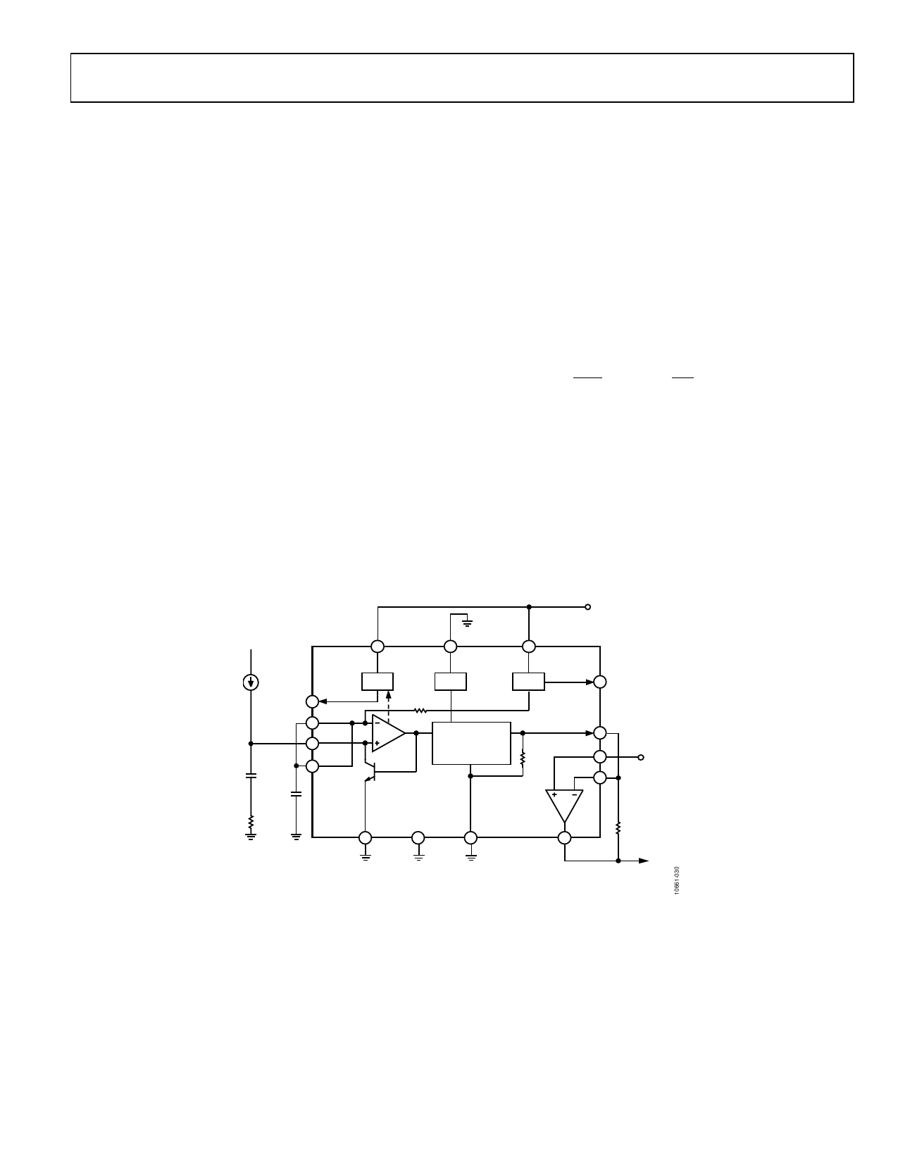
INVERTING THE SLOPE
The buffer is essentially an uncommitted op amp that can be
used to support the operation of the ADL5303 in a variety of
ways. It can be completely disconnected from the signal chain
when not needed. Figure 30 shows its use as an inverting ampli-
fier; this changes the polarity of the slope. The output can be
repositioned to a positive value by applying a fraction of VREF
to the BFIN pin. The full design for a practical application is
left undefined in this brief illustration, but a few cases are
discussed, as follows.
For example, if slope of −30 mV/dB is needed; a gain of 3 is
required. Because VLOG exhibits a source resistance of 5 kΩ,
RA must be 15 kΩ. A positive offset, VOS, is applied to the BFIN
pin, as indicated in Figure 30. The resulting output voltage can
be expressed as
VOUT
=
−
RA
5 kΩ
VY
× log10
I PD
IZ
+VOS
(11)
When the gain is set to 13 (RA = 5 kΩ), the 2 V VREF can be tied
directly to BFIN, in which case the starting point for the output
response is at 4 V. However, because the slope in this case is
only −0.2 V/decade, the full current range takes the output
down by only 1.6 V. Clearly, a higher slope (or gain) is desirable;
in which case, set VOS to a smaller voltage to avoid railing the
output at low currents. If VOS = 1.2 V and G = 33, VOUT now
starts at 4.8 V and falls through this same voltage toward ground
with a slope of −0.6 V per decade, spanning the full range of IPD.
VP
VPS2
PWDN
VPS1
10
16
12
ADL5303
IPD
VPDB
NC 5
PDB
BIAS
~10kΩ
VREF
0.5V
VREF
6 NC
C1
1nF
C3
100nF
VSUM
2
INPT
3
VSUM
4
VLOG
8
TEMPERATURE
COMPENSATION
BFIN
5kΩ
9
VOS
BFNG
13
R1
750Ω
15
GND
7
ACOM
14
GND
11
VOUT
R15 (RA)
VOUT
NC = NO CONNECT
Figure 30. Using the Buffer to Invert the Polarity of the Slope
Rev. 0 | Page 17 of 24
Share Link: 