AD8362 查看數據表(PDF) - Analog Devices
零件编号
产品描述 (功能)
生产厂家
AD8362 Datasheet PDF : 32 Pages
| |||
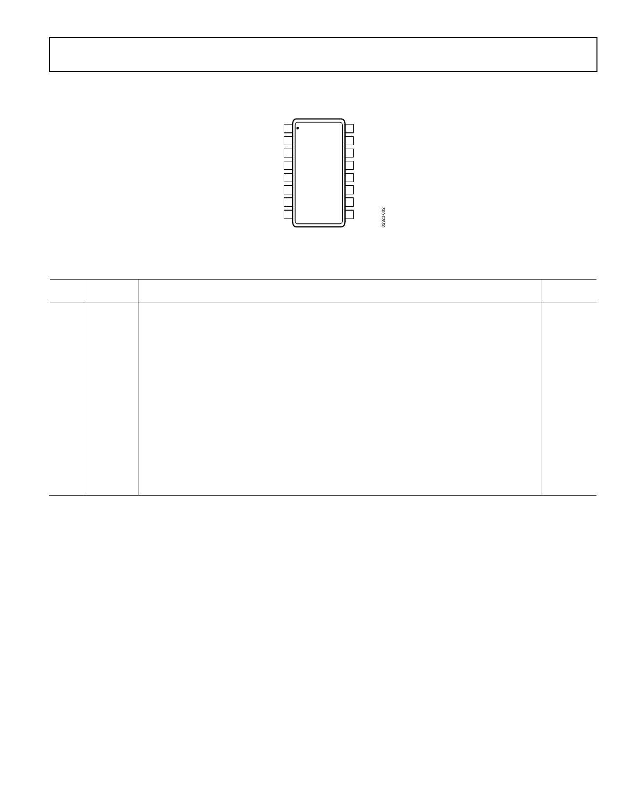
PIN CONFIGURATION AND FUNCTION DESCRIPTIONS
AD8362
COMM 1
CHPF 2
DECL 3
INHI 4
INLO 5
DECL 6
PWDN 7
COMM 8
16 ACOM
15 VREF
AD8362
TOP VIEW
(Not to Scale)
14 VTGT
13 VPOS
12 VOUT
11 VSET
10 ACOM
9 CLPF
Figure 2. Pin Configuration
Table 3. Pin Function Descriptions
Pin
No. Mnemonic Description
1, 8 COMM
Common Connection. Connect via low impedance to system common.
2
CHPF
Input HPF. Connect to common via a capacitor to determine 3 dB point of input signal high-pass filter.
3, 6 DECL
Decoupling Terminals for INHI and INLO. Connect to common via a large capacitance to complete
input circuit.
4, 5 INHI , INLO Differential Signal Input Terminals. Input Impedance = 200 Ω. Can also be driven single-ended, in
which case, the input impedance reduces to 100 Ω.
7
PWDN
Disable/Enable Control Input. Apply logic high voltage to shut down the AD8362.
9
CLPF
Connection for Ground Referenced Loop Filter Integration (Averaging) Capacitor.
10, 16 ACOM
Analog Common Connection for Output Amplifier.
11 VSET
Setpoint Input. Connect directly to VOUT for measurement mode. Apply setpoint input to this pin for
controller mode.
12 VOUT
RMS Output. In measurement mode, VOUT is normally connected directly to VSET.
13 VPOS
Connect to 5 V Power Supply.
14 VTGT
The logarithmic intercept voltage is proportional to the voltage applied to this pin. The use of a lower
target voltage increases the crest factor capacity. Normally connected to VREF.
15 VREF
General-Purpose Reference Voltage Output of 1.25 V. Usually connected only to VTGT.
Equivalent
Circuit
Circuit A
Circuit B
Circuit C
Circuit D
Circuit E
Rev. D | Page 7 of 32
Share Link: 