AD7192 查看數據表(PDF) - Analog Devices
零件编号
产品描述 (功能)
生产厂家
AD7192 Datasheet PDF : 40 Pages
| |||
AD7192
STATUS REGISTER
(RS2, RS1, RS0 = 0, 0, 0; Power-On/Reset = 0x80)
The status register is an 8-bit read-only register. To access the ADC status register, the user must write to the communications register,
select the next operation to be a read, and load Bit RS2, Bit RS1, and Bit RS0 with 0. Table 16 outlines the bit designations for the status
register. SR0 through SR7 indicate the bit locations, SR denoting that the bits are in the status register. SR7 denotes the first bit of the data
stream. The number in parentheses indicates the power-on/reset default status of that bit.
SR7
RDY(1)
SR6
ERR(0)
SR5
SR4
SR3
NOREF(0)
PARITY(0)
0(0)
SR2
CHD2(0)
SR1
CHD1(0)
SR0
CHD0(0)
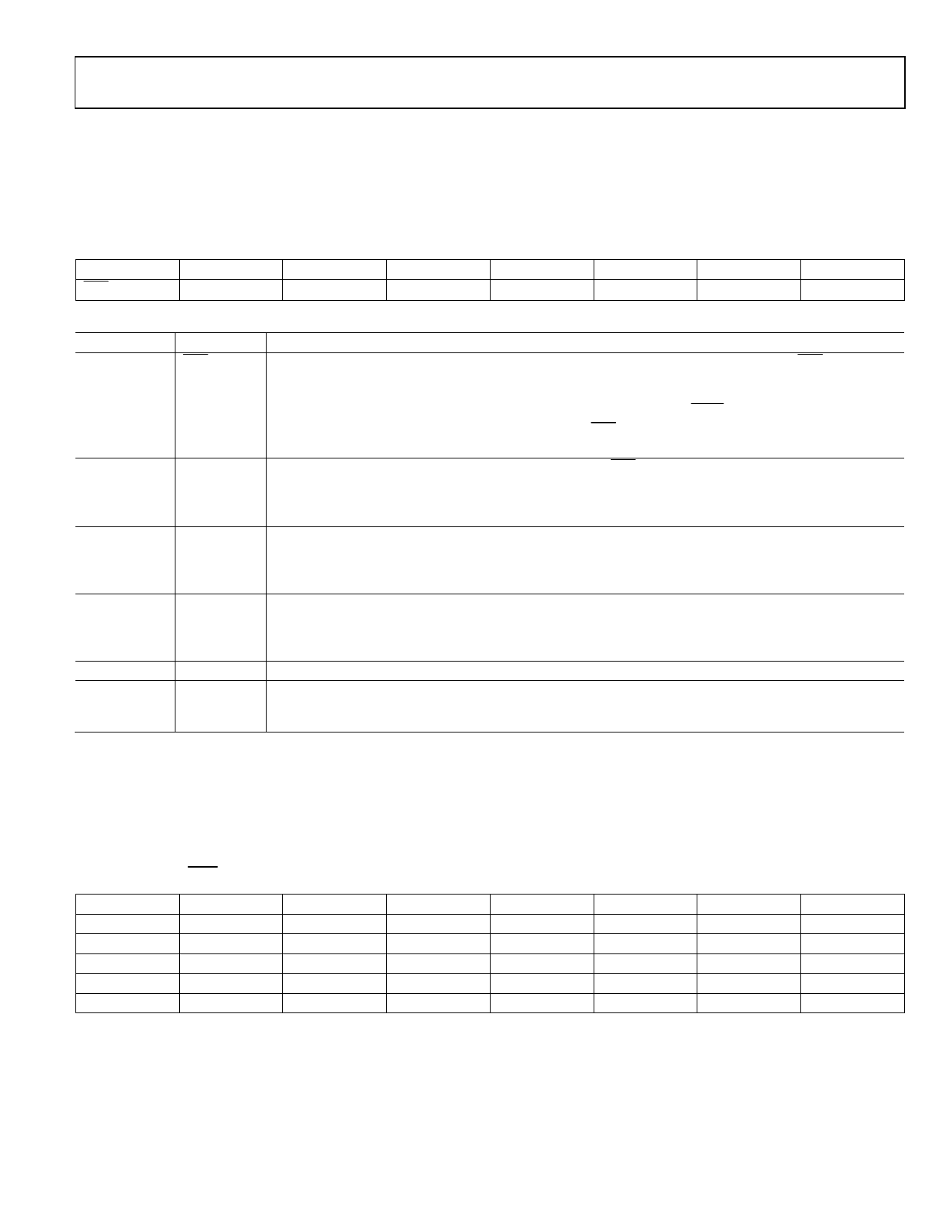
Table 16. Status Register Bit Designations
Bit Location Bit Name Description
SR7
RDY
Ready bit for the ADC. This bit is cleared when data is written to the ADC data register. The RDY bit is set
automatically after the ADC data register is read, or a period of time before the data register is updated,
with a new conversion result to indicate to the user that the conversion data should not be read. It is also
set when the part is placed in power-down mode or idle mode or when SYNC is taken low.
The end of a conversion is also indicated by the DOUT/RDY pin. This pin can be used as an alternative to
the status register for monitoring the ADC for conversion data.
SR6
ERR
ADC error bit. This bit is written to at the same time as the RDY bit. This bit is set to indicate that the result
written to the ADC data register is clamped to all 0s or all 1s. Error sources include overrange or under-
range or the absence of a reference voltage. This bit is cleared when the result written to the data register is
within the allowed analog input range again.
SR5
NOREF
No external reference bit. This bit is set to indicate that the selected reference (REFIN1 or REFIN2) is at a
voltage that is below a specified threshold. When set, conversion results are clamped to all 1s. This bit is
cleared to indicate that a valid reference is applied to the selected reference pins. The NOREF bit is enabled
by setting the REFDET bit in the configuration register to 1.
SR4
PARITY
Parity check of the data register. If the ENPAR bit in the mode register is set, the PARITY bit is set if there is
an odd number of 1s in the data register. It is cleared if there is an even number of 1s in the data register.
The DAT_STA bit in the mode register should be set when the parity check is used. When the DAT_STA bit is
set, the contents of the status register are transmitted along with the data for each data register read.
SR3
0
This bit is set to 0.
SR2 to SR0
CHD2 to
CHD0
These bits indicate which channel corresponds to the data register contents. They do not indicate which
channel is presently being converted but indicate which channel was selected when the conversion
contained in the data register was generated.
MODE REGISTER
(RS2, RS1, RS0 = 0, 0, 1; Power-On/Reset = 0x080060)
The mode register is a 24-bit register from which data can be read or to which data can be written. This register is used to select the
operating mode, the output data rate, and the clock source. Table 17 outlines the bit designations for the mode register. MR0 through
MR23 indicate the bit locations, MR denoting that the bits are in the mode register. MR23 denotes the first bit of the data stream. The
number in parentheses indicates the power-on/reset default status of that bit. Any write to the mode register resets the modulator and
filter and sets the RDY bit.
MR23
MD2(0)
MR15
SINC3(0)
MR7
FS7(0)
MR22
MD1(0)
MR14
0
MR6
FS6(1)
MR21
MD0(0)
MR13
ENPAR(0)
MR5
FS5(1)
MR20
DAT_STA(0)
MR12
CLK_DIV(0)
MR4
FS4(0)
MR19
CLK1(1)
MR11
SINGLE(0)
MR3
FS3(0)
MR18
CLK0(0)
MR10
REJ60(0)
MR2
FS2(0)
MR17
0
MR9
FS9(0)
MR1
FS1(0)
MR16
0
MR8
FS8(0)
MR0
FS0(0)
Rev. A | Page 19 of 40
Share Link: 