79C2040RPFE-20 查看數據表(PDF) - MAXWELL TECHNOLOGIES
零件编号
产品描述 (功能)
生产厂家
79C2040RPFE-20 Datasheet PDF : 17 Pages
| |||
20 Megabit (512 x 40-Bit) EEPROM MCM
79C2040
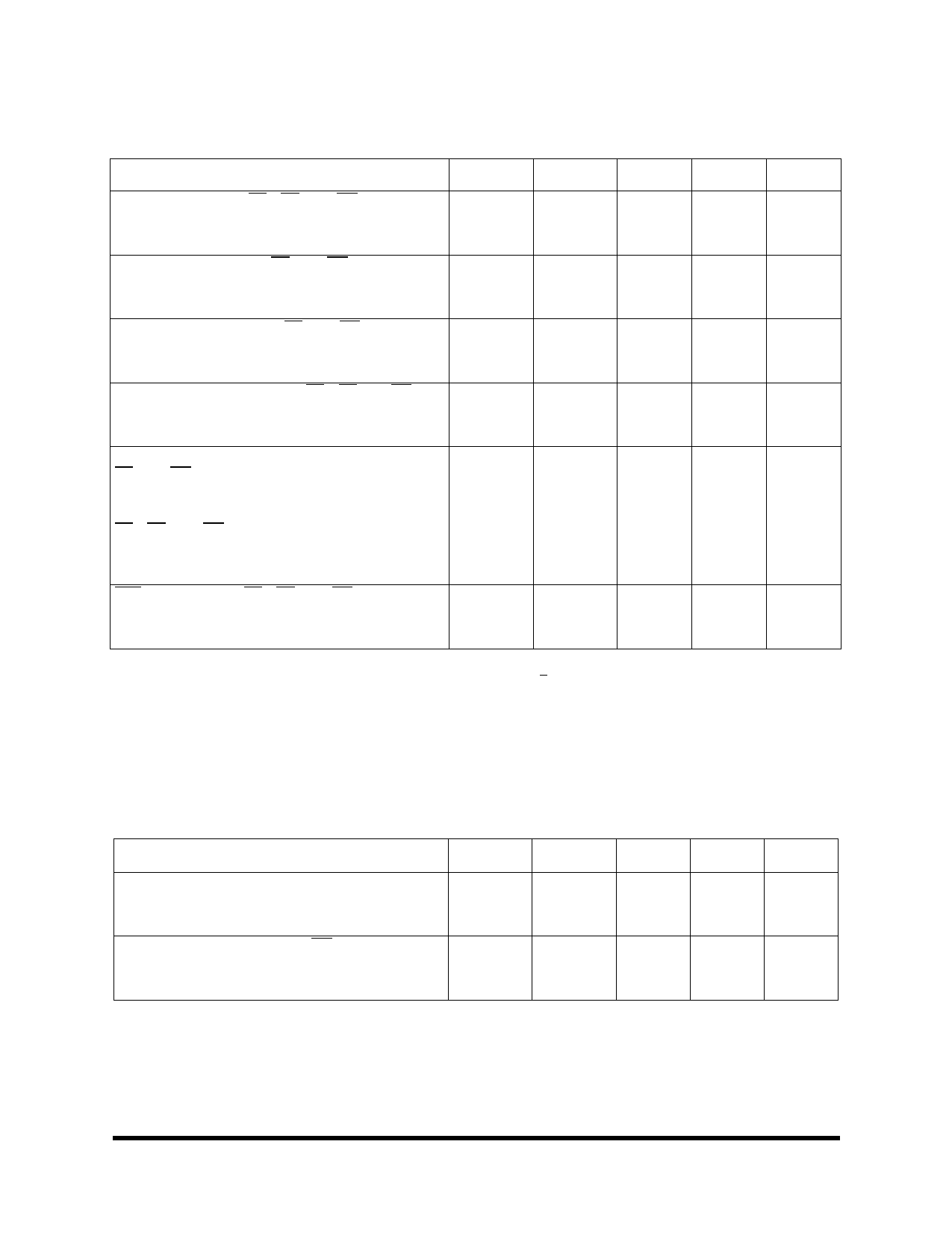
TABLE 6. 79C2040 AC ELECTRICAL CHARACTERISTICS FOR READ OPERATION 1
(V
CC
=
5V
±
10%,
TA
=
-55
TO
+125°
C)
PARAMETER
SYMBOL
SUBGROUPS
MIN
MAX
UNIT
Address Access Time CE = OE = VIL, WE = VIH
-150
-200
tACC
9, 10, 11
ns
--
150
--
200
Chip Enable Access Time OE = VIL, WE = VIH
-150
-200
tCE
9, 10, 11
ns
--
150
--
200
Output Enable Access TIme CE = VIL, WE = VIH
-150
-200
tOE
9, 10, 11
ns
0
75
0
100
Output Hold to Address Change CE = OE =VIL, WE = VIH
tOH
9, 10, 11
ns
-150
0
--
-200
0
--
Output Disable to High-Z 2
CE = VIL, WE = VIH
-150
-200
CE = OE = VIL, WE = VIH
-150
-200
9, 10, 11
tDF
ns
0
50
0
60
tDFR
ns
0
350
0
450
RES to Output Delay CE = OE = VIL, WE = VIH3
-150
-200
TRR
9, 10, 11
ns
0
450
0
650
1. Test conditions: input pulse levels = 0.4V to 2.4V; input rise and fall times < 20 ns; output load = 1 TTL gate + 100 pF (including
scope and fixture); reference levels for measuring timing = 0.8 V/1.8 V.
2. tDF and tDFR are defined as the time at which the output becomes an open circuit and data is no longer driven.
3. Guaranteed by design.
PARAMETER
TABLE 7. 79C2040 AC ELECTRICAL CHARACTERISTICS FOR WRITE OPERATION
(V
CC
=
5V
±
10%,
TA
=
-55
TO
+125°
C)
SYMBOL
SUBGROUPS
MIN 1
MAX
UNITS
Address Setup Time
-150
-200
tAS
9, 10, 11
0
0
ns
--
--
Chip Enable to Write Setup Time (WE controlled)
-150
-200
tCS
9, 10, 11
0
0
ns
--
--
04.20.05 Rev 1
All data sheets are subject to change without notice 5
©2005 Maxwell Technologies
All rights reserved
Share Link: 