74LVC1G57GV 查看數據表(PDF) - Philips Electronics
零件编号
产品描述 (功能)
生产厂家
74LVC1G57GV Datasheet PDF : 18 Pages
| |||
Philips Semiconductors
74LVC1G57
Low-power configurable multiple function gate
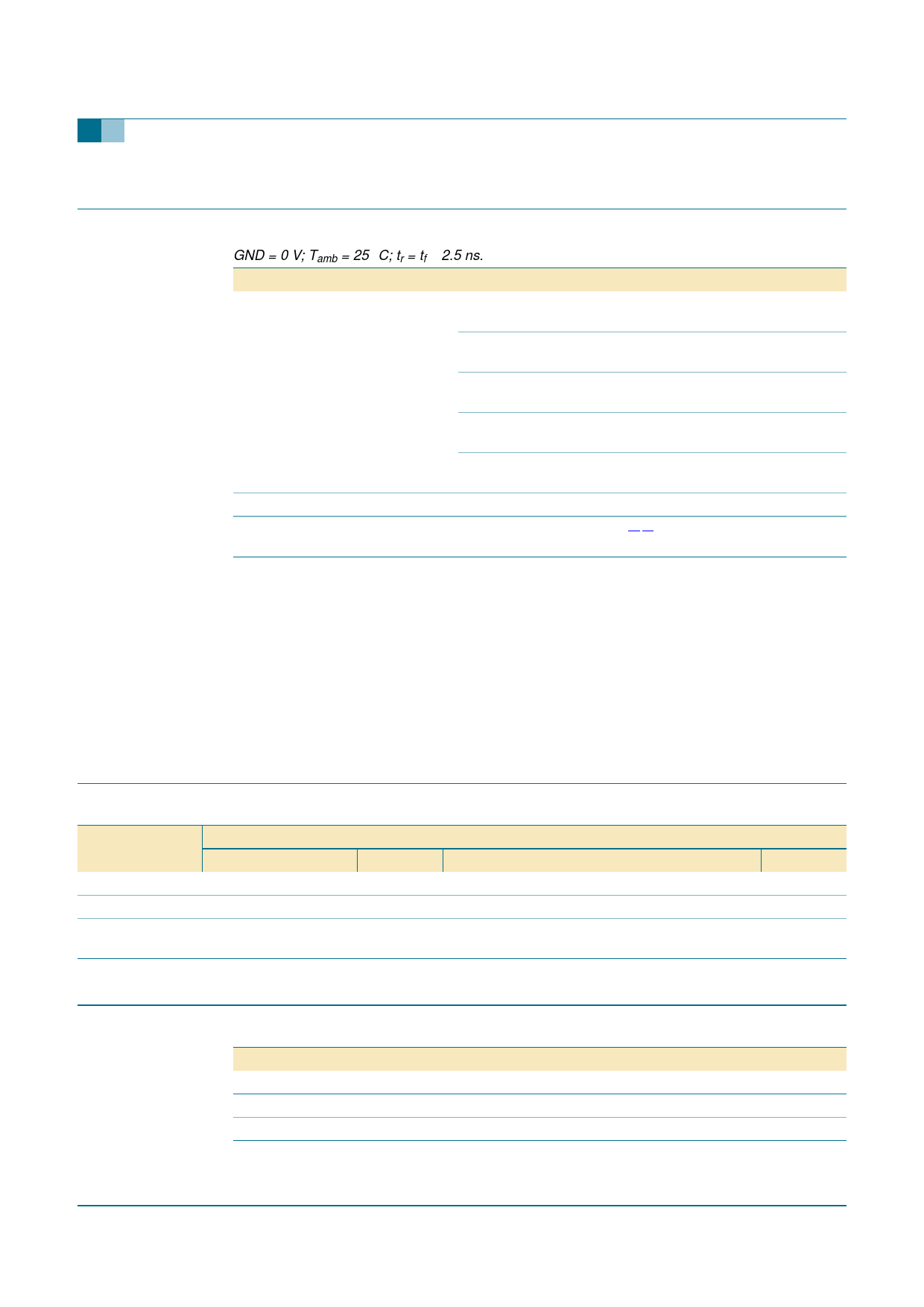
3. Quick reference data
Table 1: Quick reference data
GND = 0 V; Tamb = 25 °C; tr = tf ≤ 2.5 ns.
Symbol Parameter
Conditions
Min Typ Max Unit
tPHL, tPLH propagation delay
input A, B and
C to output Y
CL = 30 pF; RL = 1 kΩ;
VCC = 1.8 V
CL = 30 pF; RL = 500 Ω;
VCC = 2.5 V
CL = 50 pF; RL = 500 Ω;
VCC = 2.7 V
CL = 50 pF; RL = 500 Ω;
VCC = 3.3 V
CL = 50 pF; RL = 500 Ω;
VCC = 5.0 V;
-
6.0 -
ns
-
3.5 -
ns
-
4.2 -
ns
-
3.8 -
ns
-
3.0 -
ns
CI
input capacitance
CPD
power dissipation
VCC = 3.3 V
capacitance per buffer
-
2.5 -
pF
[1] [2] -
22 -
pF
[1] CPD is used to determine the dynamic power dissipation (PD in µW).
PD = CPD × VCC2 × fi × N + Σ(CL × VCC2 × fo) where:
fi = input frequency in MHz;
fo = output frequency in MHz;
CL = output load capacitance in pF;
VCC = supply voltage in V;
N = total load switching outputs;
Σ(CL × VCC2 × fo) = sum of the outputs.
[2] The condition is VI = GND to VCC.
4. Ordering information
Table 2: Ordering information
Type number
Package
Temperature range
74LVC1G57GW −40 °C to +125 °C
74LVC1G57GV −40 °C to +125 °C
74LVC1G57GM −40 °C to +125 °C
Name
-
-
XSON6
5. Marking
Description
plastic surface mounted package; 6 leads
plastic surface mounted package; 6 leads
plastic extremely thin small outline package;
no leads; 6 terminals; body 1 × 1.45 × 0.5 mm
Version
SOT363
SOT457
SOT886
Table 3: Marking
Type number
74LVC1G57GW
74LVC1G57GV
74LVC1G57GM
Marking code
YC
V57
YC
9397 750 13722
Product data sheet
Rev. 01 — 6 September 2004
© Koninklijke Philips Electronics N.V. 2004. All rights reserved.
2 of 18
Share Link: 