74LVC126ADB 查看數據表(PDF) - Philips Electronics
零件编号
产品描述 (功能)
生产厂家
74LVC126ADB Datasheet PDF : 20 Pages
| |||
Philips Semiconductors
Quad buffer/line driver with 5 Volt
tolerant input/outputs; 3-state
Product specification
74LVC126A
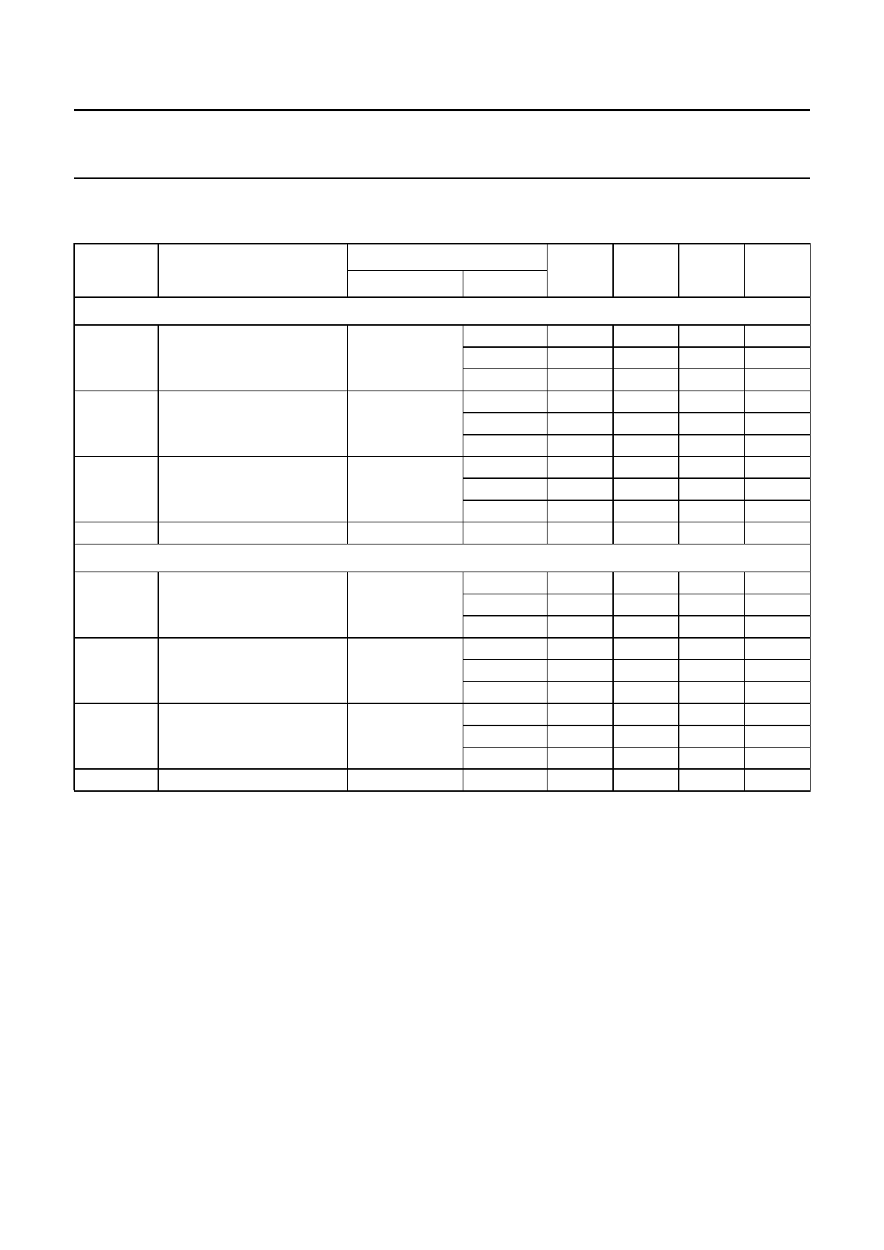
AC CHARACTERISTICS
GND = 0 V; tr = tf ≤ 2.5 ns.
SYMBOL
PARAMETER
Tamb = −40 to +85 °C
tPHL/tPLH propagation delay nA to nY
tPZH/tPZL
3-state output enable time
nOE to nY
tPHZ/tPLZ
3-state output disable time
nOE to nY
tsk(0)
skew
Tamb = −40 to +125 °C
tPHL/tPLH propagation delay nA to nY
tPZH/tPZL
3-state output enable time
nOE to nY
tPHZ/tPLZ
3-state output disable time
nOE to nY
tsk(0)
skew
TEST CONDITIONS
WAVEFORMS VCC (V)
see Figs 6 and 8 1.2
2.7
3.0 to 3.6
see Figs 7 and 8 1.2
2.7
3.0 to 3.6
see Figs 7 and 8 1.2
2.7
3.0 to 3.6
note 3
3.0 to 3.6
see Figs 6 and 8 1.2
2.7
3.0 to 3.6
see Figs 7 and 8 1.2
2.7
3.0 to 3.6
see Figs 7 and 8 1.2
2.7
3.0 to 3.6
note 3
3.0 to 3.6
MIN.
−
1.5
1.0
−
1.5
1.0
−
1.5
1.3
−
−
1.5
1.0
−
1.5
1.0
−
1.5
1.3
−
TYP.(1) MAX. UNIT
11
−
ns
2.7
5.2
ns
2.4(2)
4.7
ns
15
−
ns
3.1
6.3
ns
2.9(2)
5.7
ns
8.0
−
ns
3.8
6.7
ns
2.8(2)
6.0
ns
−
1.0
ns
−
−
ns
−
6.5
ns
−
6.0
ns
−
−
ns
−
8.0
ns
−
7.5
ns
−
−
ns
−
8.5
ns
−
7.5
ns
−
1.5
ns
Notes
1. Typical values are measured at Tamb = 25 °C.
2. Typical values are measured at VCC = 3.3 V.
3. Skew between any two outputs of the same package switching in the same direction. This parameter is guaranteed
by design.
2003 Feb 28
8
Share Link: 