74F280SC 查看數據表(PDF) - Fairchild Semiconductor
零件编号
产品描述 (功能)
生产厂家
74F280SC Datasheet PDF : 6 Pages
| |||
Unit Loading/Fan Out
Pin Names Description
I0–I8
∑O
∑E
Data Inputs
Odd Parity Output
Even Parity Output
U.L.
HIGH/LOW
1.0/1.0
50/33.3
50/33.3
Input IIH/IIL
Output IOH/IOL
20 µA/−0.6 mA
−1 mA/20 mA
−1 mA/20 mA
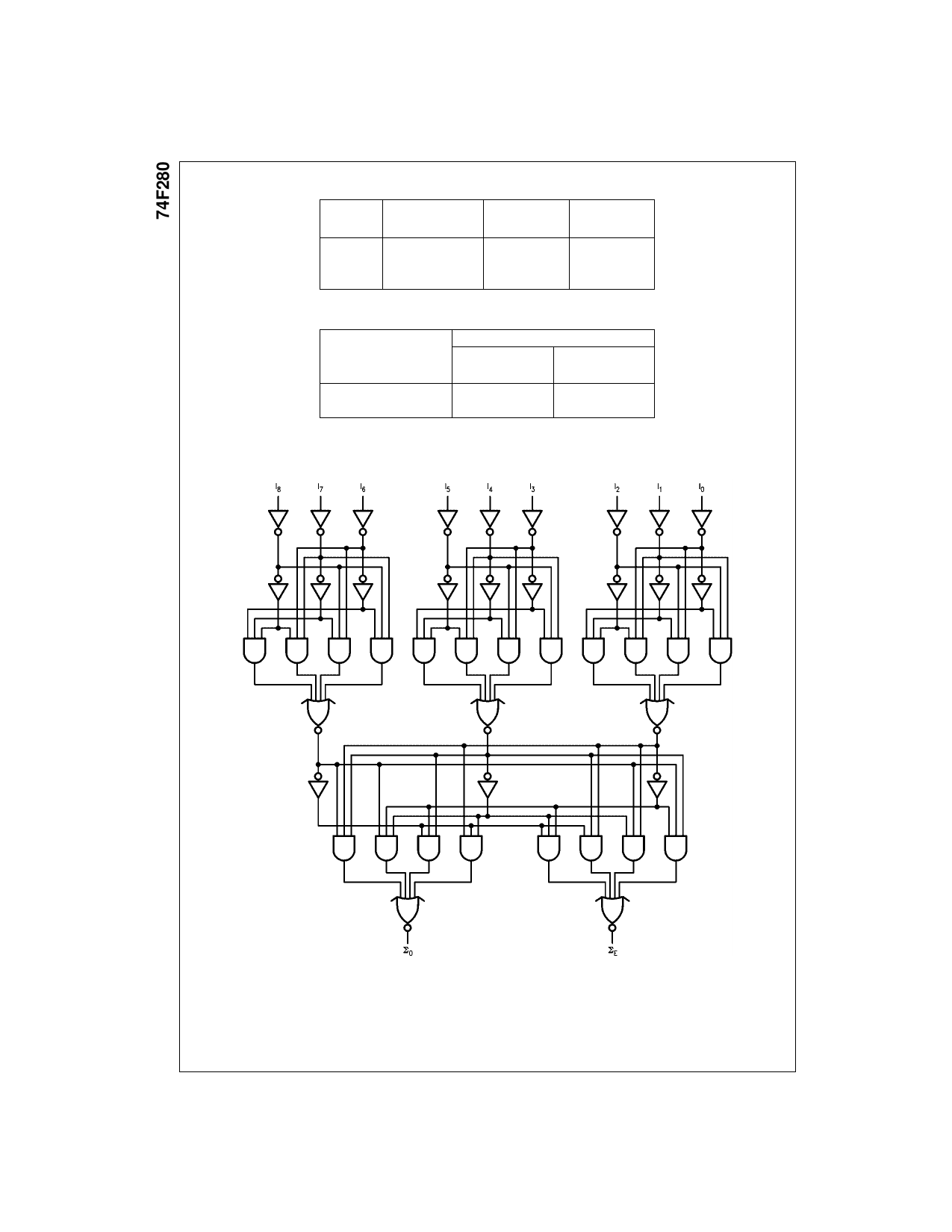
Truth Table
H = HIGH Voltage Level
L = LOW Voltage Level
Number of
HIGH Inputs
I0–I8
0, 2, 4, 6, 8
1, 3, 5, 7, 9
Outputs
∑ Even
∑ Odd
H
L
L
H
Logic Diagram
Please note that this diagram is provided only for the understanding of logic operations and should not be used to estimate propagation delays.
www.fairchildsemi.com
2
Share Link: 