74ALVCH16825 查看數據表(PDF) - Philips Electronics
零件编号
产品描述 (功能)
生产厂家
74ALVCH16825 Datasheet PDF : 10 Pages
| |||
Philips Semiconductors
18-bit buffer/driver (3-State)
Product specification
74ALVCH16825
FEATURES
• Wide supply voltage range of 1.2V to 3.6V
• Complies with JEDEC standard no. 8-1A.
• CMOS low power consumption
• Direct interface with TTL levels
• Current drive ± 24 mA at 3.0 V
• MULTIBYTETM flow-through standard pin-out architecture
• Low inductance multiple VCC and GND pins for minimum noise
and ground bounce
• All data inputs have bus hold
• Output drive capability 50Ω transmission lines @ 85°C
DESCRIPTION
The 74ALVCH16825 is an 18–bit non-inverting buffer/driver with
3-State outputs for bus-oriented applications.
The 74ALVCH16825 consists of two 9-bit sections with separate
output enable signals. For either 9-bit buffer section, the two output
enable (1OE1 and 1OE2 or 2OE1 and 2OE2) inputs must both be
LOW for corresponding D outputs to be active. If either output
enable input is HIGH, the outputs of that 9-buffer section are in the
high impedance state.
The 74ALVCH16825 has active bus hold circuitry which is provided
to hold unused or floating data inputs at a valid logic level. This
feature eliminates the need for external pull-up or pull-down
resistors.
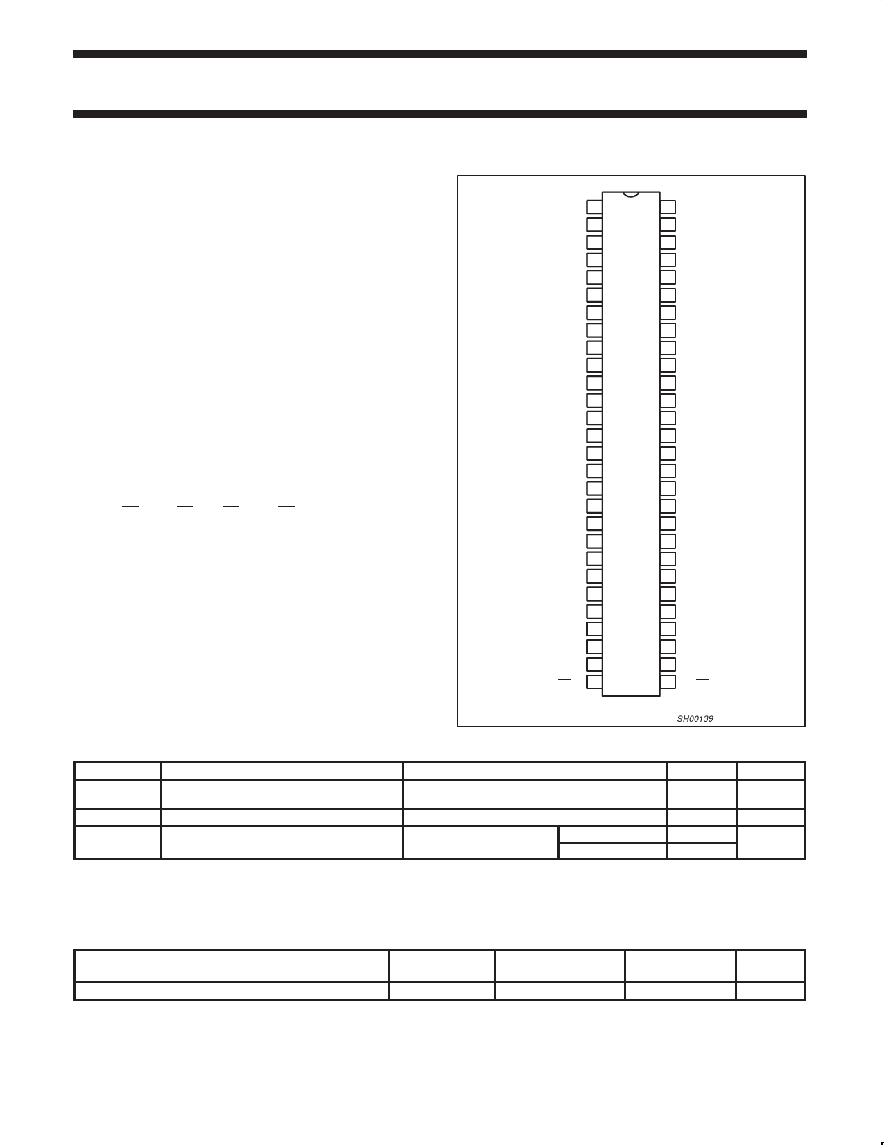
PIN CONFIGURATION
1OE1 1
1Y1 2
1Y1 3
GND 4
1Y2 5
1Y3 6
VCC 7
1Y4 8
1Y5 9
1Y6 10
GND 11
1Y7 12
1Y8 13
GND 14
GND 15
2Y0 16
2Y1 17
GND 18
2Y2 19
2Y3 20
2Y4 21
VCC 22
2Y5 23
2Y6 24
GND 25
2Y7 26
2Y8 27
2OE1 28
56 1OE2
55 1A0
54 1A1
53 GND
52 1A2
51 1A3
50 VCC
49 1A4
48 1A5
47 1A6
46 GND
45 1A7
44 1A8
43 GND
42 GND
41 2A0
40 2A1
39 GND
38 2A2
37 2A3
36 2A4
35 VCC
34 2A5
33 2A6
32 GND
31 2A7
30 2A8
29 2OE2
SH00139
QUICK REFERENCE DATA
GND = 0V; Tamb = 25°C; tr = tf ≤ 2.5ns
SYMBOL
PARAMETER
CONDITIONS
TYPICAL
tPHL/tPLH
CI
CPD
Propagation delay
CP to Qn
Input capacitance
Power dissipation capacitance per latch
VCC = 2.5V, CL = 30pF
VCC = 3.3V, CL = 50pF
VI = GND to VCC1
2.0
2.0
4.0
Output enabled
19
Output disabled
3
NOTES:
1. CPD is used to determine the dynamic power dissipation (PD in µW):
PD = CPD × VCC2 × fi + S (CL × VCC2 × fo) where: fi = input frequency in MHz; CL = output load capacitance in pF;
fo = output frequency in MHz; VCC = supply voltage in V; S (CL × VCC2 × fo) = sum of outputs.
UNIT
ns
pF
pF
ORDERING INFORMATION
PACKAGES
56-Pin Plastic Thin Shrink Small Outline (TSSOP) Type II
TEMPERATURE
RANGE
–40°C to +85°C
OUTSIDE NORTH
AMERICA
74ALVCH16825 DGG
NORTH AMERICA
ACH16825 DGG
DRAWING
NUMBER
SOT364-1
1998 Jul 27
2
853-2097 19785
Share Link: 