74ALVC00BQ 查看數據表(PDF) - Philips Electronics
零件编号
产品描述 (功能)
生产厂家
74ALVC00BQ Datasheet PDF : 16 Pages
| |||
Philips Semiconductors
Quad 2-input NAND gate
Product specification
74ALVC00
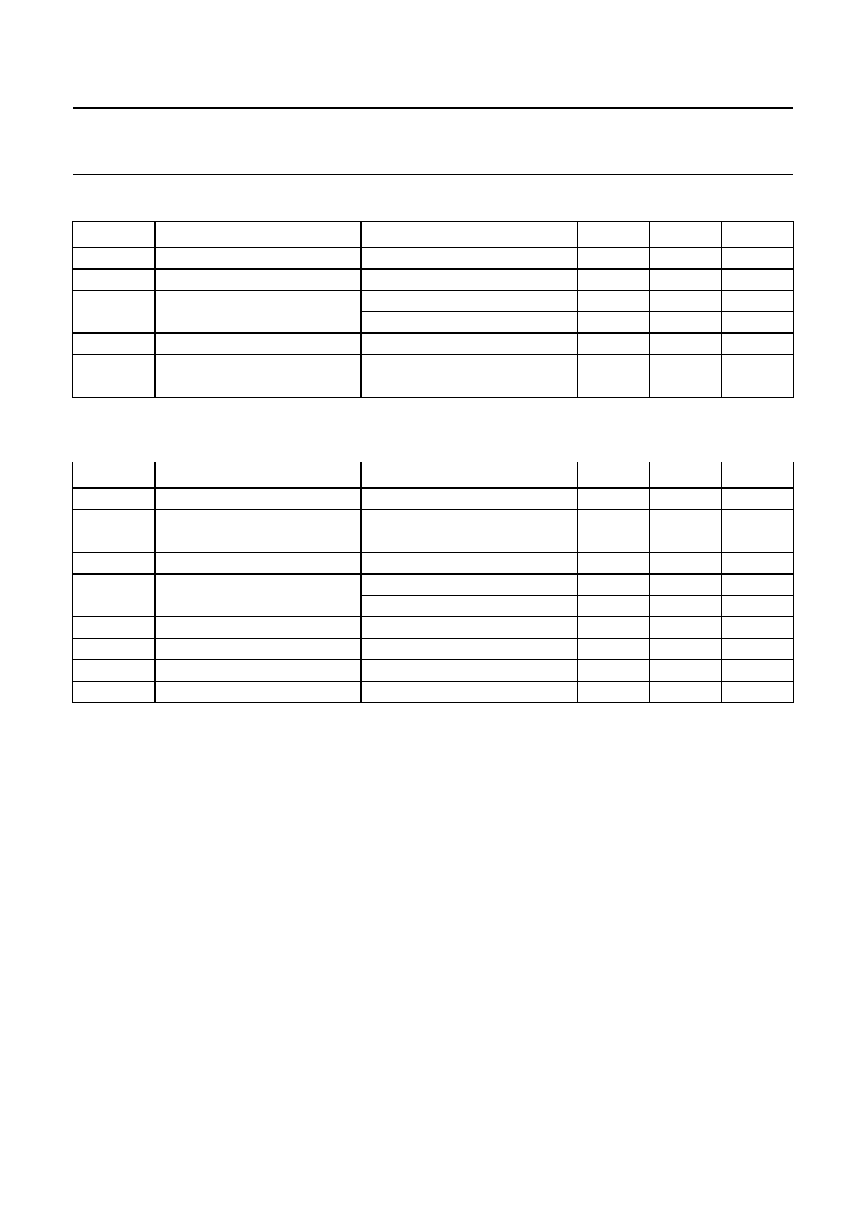
RECOMMENDED OPERATING CONDITIONS
SYMBOL
VCC
VI
VO
Tamb
tr, tf
PARAMETER
supply voltage
input voltage
output voltage
operating ambient temperature
input rise and fall times
CONDITIONS
VCC = 1.65 to 3.6 V
VCC = 0 V; Power-down mode
VCC = 1.65 to 2.7 V
VCC = 2.7 to 3.6 V
MIN.
1.65
0
0
0
−40
0
0
MAX.
3.6
3.6
VCC
3.6
+85
20
10
UNIT
V
V
V
V
°C
ns/V
ns/V
LIMITING VALUES
In accordance with the Absolute Maximum Rating System (IEC 60134); voltages are referenced to GND (ground = 0 V).
SYMBOL
VCC
IIK
VI
IOK
VO
PARAMETER
supply voltage
input diode current
input voltage
output diode current
output voltage
IO
ICC, IGND
Tstg
Ptot
output source or sink current
VCC or GND current
storage temperature
power dissipation per package
CONDITIONS
VI < 0
VO > VCC or VO < 0
notes 1 and 2
Power-down mode; note 2
VO = 0 to VCC
Tamb = −40 to +125 °C; note 3
MIN.
−0.5
−
−0.5
−
−0.5
−0.5
−
−
−65
−
MAX.
UNIT
+4.6
V
−50
mA
+4.6
V
±50
mA
VCC + 0.5 V
+4.6
V
±50
mA
±100
mA
+150
°C
500
mW
Notes
1. The input and output voltage ratings may be exceeded if the input and output current ratings are observed.
2. When VCC = 0 V (Power-down mode), the output voltage can be 3.6 V in normal operation.
3. For SO14 packages: above 70 °C derate linearly with 8 mW/K.
For TSSOP14 packages: above 60 °C derate linearly with 5.5 mW/K.
For DHVQFN14 packages: above 60 °C derate linearly with 4.5 mW/K.
2003 May 14
5
Share Link: 