100315 查看數據表(PDF) - Fairchild Semiconductor
零件编号
产品描述 (功能)
生产厂家
100315 Datasheet PDF : 4 Pages
| |||
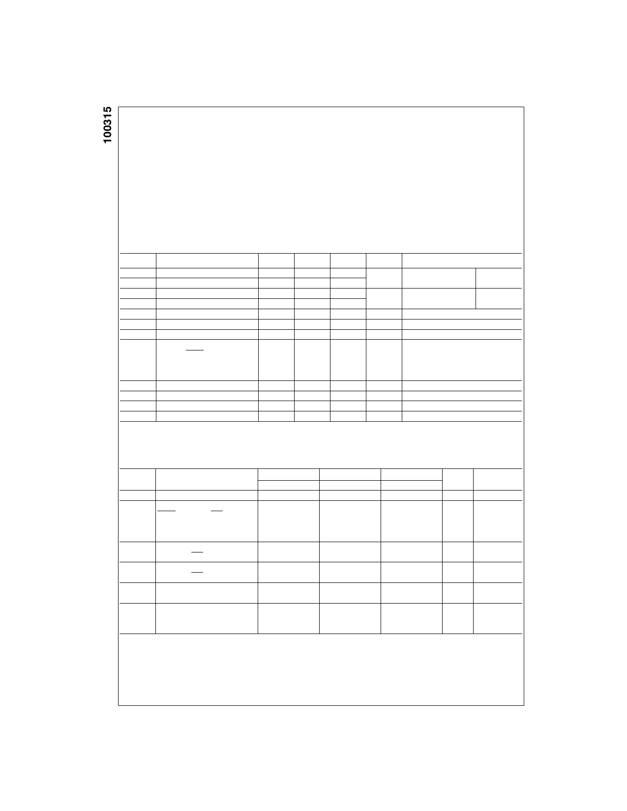
Absolute Maximum Ratings(Note 2)
Storage Temperature
Maximum Junction Temperature (TJ)
Case Temperature under Bias (TC)
VEE Pin Potential to Ground Pin
Input Voltage (DC)
Output Current (DC Output HIGH)
Operating Range (Note 2)
ESD (Note 3)
−65°C to +150°C
+150°C
0°C to +85°C
−7.0V to +0.5V
VCC to +0.5V
−50 mA
−5.7V to −4.2V
≥2000V
Recommended Operating
Conditions
Case Temperature (TC)
0°C to +85°C
Supply Voltage (VEE)
−5.7V to −4.2V
Note 2: The “Absolute Maximum Ratings” are those values beyond which
the safety of the device cannot be guaranteed. The device should not be
operated at these limits. The parametric values defined in the Electrical
Characteristics tables are not guaranteed at the absolute maximum rating.
The “Recommended Operating Conditions” table will define the conditions
for actual device operation.
Note 3: ESD testing conforms to MIL-STD-883, Method 3015.
DC Electrical Characteristics (Note 4)
VEE = −4.2V to −5.7V, VCC = VCCA = GND, TC = 0°C to +85°C
Symbol
Parameter
Min
Typ
Max
Units
Conditions
VOH
VOL
VOHC
VOLC
VIH
VIL
IIL
IIH
Output HIGH Voltage
Output LOW Voltage
Output HIGH Voltage
Output LOW Voltage
Single-Ended Input HIGH Voltage
Single-Ended Input LOW Voltage
Input LOW Current
Input HIGH Current
CLKIN, CLKIN
TCLK
−1025
−1830
−1035
−1165
−1830
0.50
−955
−1705
−870
−1620
−1610
−870
−1475
150
250
mV
VIN = VIH(Max)
Loading with
or VIL(Min)
50Ω to −2.0V
mV
VIN = VIH(Min)
Loading with
or VIL(Max)
50Ω to −2.0V
mV Guaranteed HIGH Signal for All Inputs
mV Guaranteed LOW Signal for All Inputs
µA
VIN = VIL(Min)
µA
µA
VIN = VIH(Max)
CLKSEL
250
µA
VDIFF
Input Voltage Differential
150
mV Required for Full Output Swing
VCM
Common Mode Voltage
VCC − 2V
VCC − 0.5V
V
ICBO
Input Leakage Current
−10
µA
VIN = VEE
IEE
Power Supply Current
−67
−35
mA
Note 4: The specified limits represent the “worst case” value for the parameter. Since these “worst case” values normally occur at the temperature extremes,
additional noise immunity and guard banding can be achieved by decreasing the allowable system operating ranges.
AC Electrical Characteristics
VEE = −4.2V to −4.8, VCC = VCCA = GND
Symbol
Parameter
TC = 0°C
Min
Max
TC = +25°C
Min
Max
TC = +85°C
Min
Max
Units
Conditions
fMAX
tPLH
tPHL
Maximum Clock Frequency
Propagation Delay CLKIN,
CLKIN to CLK(1–4), CLK(1–4)
Differential
750
0.59
0.79
750
0.62
0.82
750
0.67
0.87
MHz
ns Figures 1, 3
Single-Ended 0.59
0.99
0.62
1.02
0.67
1.07
tPLH
tPHL
tPLH
tPHL
tTLH
tTHL
tOST
DIFF
Propagation Delay, TCLK
to CLK(1–4), CLK(1–4)
Propagation Delay, CLKSEL
to CLK(1–4), CLK(1–4)
Transition Time
20% to 80%, 80% to 20%
Maximum Skew Opposite Edge
Output-to-Output Variation
0.50
0.80
0.30
1.20
1.60
0.80
0.50
0.80
0.30
1.20
1.60
0.80
0.50
0.80
0.30
1.20
1.60
0.80
ns Figures 1, 2
ns Figures 1, 2
ns Figures 1, 4
50
50
50
ps (Note 5)
Data to Output Path
Note 5: Output-to-Output Skew is defined as the absolute value of the difference between the actual propagation delay for any outputs within the same pack-
aged device. The specifications apply to any outputs switching in the same direction either HIGH-to-LOW (tOSHL), or LOW-to-HIGH (tOSLH), or in opposite
directions both HL and LH (tOST). Parameters tOST and tPS guaranteed by design.
www.fairchildsemi.com
2
Share Link: 