2SD1418 查看數據表(PDF) - Renesas Electronics
零件编号
产品描述 (功能)
生产厂家
2SD1418 Datasheet PDF : 6 Pages
| |||
2SD1418
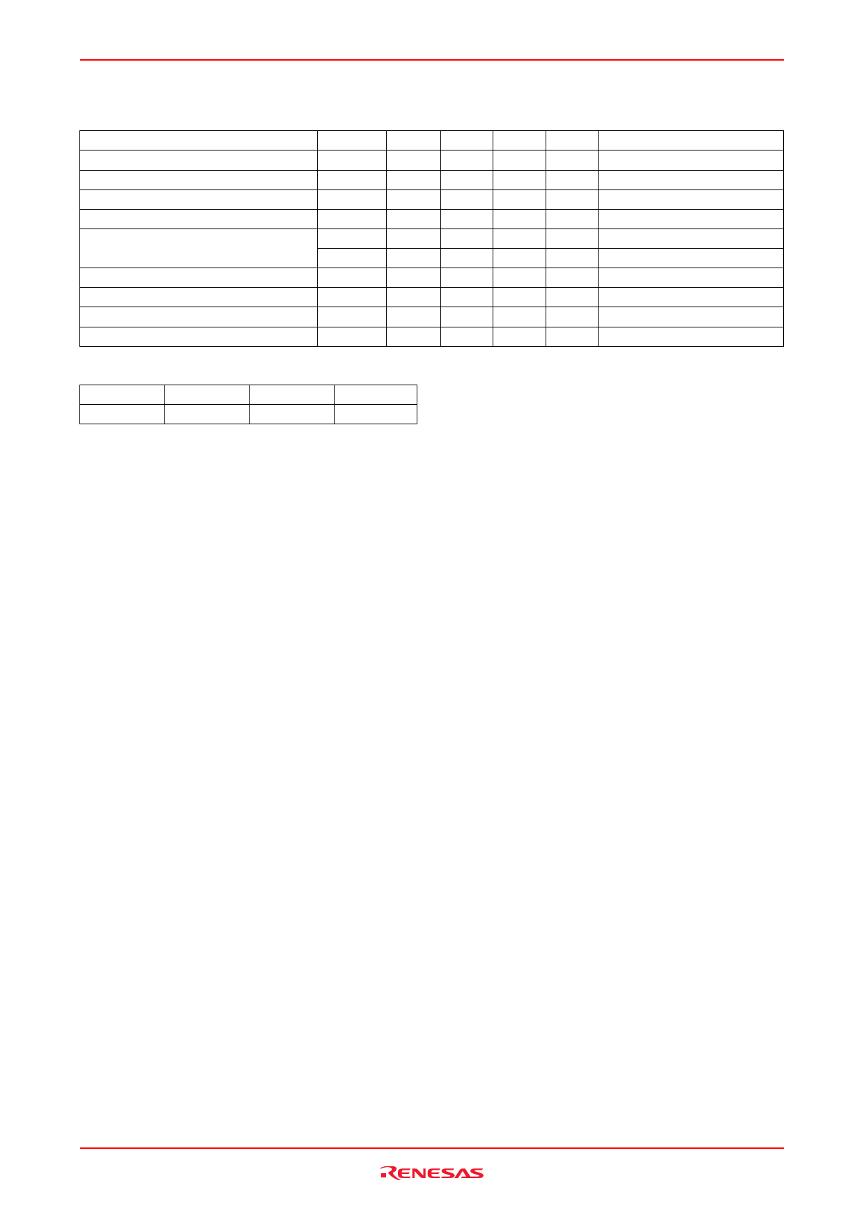
Electrical Characteristics
(Ta = 25°C)
Item
Symbol Min Typ Max Unit
Test conditions
Collector to base breakdown voltage
V(BR)CBO
120
—
—
V IC = 10 µA, IE = 0
Collector to emitter breakdown voltage V(BR)CEO
80
—
—
V IC = 1 mA, RBE = ∞
Emitter to base breakdown voltage
V(BR)EBO
5
—
—
V IE = 10 µA, IC = 0
Collector cutoff current
ICBO
—
—
10
µA VCB = 100 V, IE = 0
DC current transfer ratio
hFE1*1
60
—
320
VEB = 5 V, IC = 150 mA*2
hFE2
30
—
—
VCE = 5 V, IC = 500 mA*2
Collector to emitter saturation voltage
VCE(sat)
—
—
1
V IC = 500 mA, IB = 50 mA*2
Base to emitter voltage
VBE
—
—
1.5
V VCE = 5 V, IC = 150 mA*2
Gain bandwidth product
fT
—
140
—
MHz VCE = 5 V, IC = 150 mA*2
Collector output capacitance
Cob
—
12
—
pF VCB = 10 V, IE = 0, f = 1 MHz
Notes: 1. The 2SD1418 is grouped by hFE1 as follows.
2. Pulse test
Mark
DA
DB
DC
hFE1
60 to 120 100 to 200 160 to 320
Rev.2.00 Aug 10, 2005 page 2 of 5
Share Link: 