AN221D04-DEVLP 查看數據表(PDF) - Unspecified
零件编号
产品描述 (功能)
生产厂家
AN221D04-DEVLP Datasheet PDF : 21 Pages
| |||
AN221E04 Datasheet – Dynamically Reconfigurable FPAA With Enhanced I/O
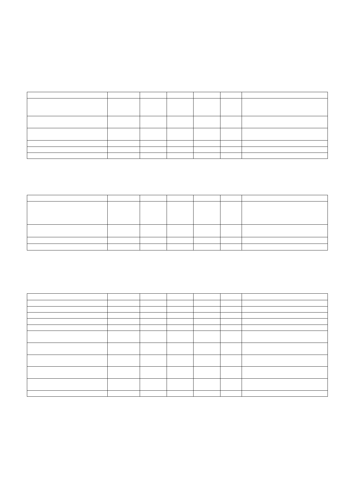
ELECTRICAL CHARACTERISTICS
Absolute Maximum Ratings
Parameter
Symbol
Min
Typ
Max Unit Comment
DC Power Supplies
AVDD(2)
BVDD
-0.5
DVDD
-
5.5 V
V
AVSS, BVSS, DVSS and SVSS all
held to 0.0 V a
xVDD to xVDD Offset
-0.5
0.5
V
Ideally all supplies should be at the
same voltage
Package Power Dissipation
Pmax 25°C
Pmax 85°C
-
-
1.8
0.73
W
Still air, No heatsink, 4 layer board,
44 pins. θja = 55°C/W
Analog and Digital Input Voltage Vinmax Vss-0.5
-
Vdd+0.5 V
Ambient Operating Temperature
Top
-40
-
85
°C
Storage Temperature
Tstg
-65
150
°C
a Absolute Maximum DC Power Supply Rating - The failure mode is non-catastrophic for Vdd of up to 7 volts, but will cause reduced
operating life time. The additional stress caused by higher local electric fields within the CMOS circuitry may induce metal migration,
oxide leakage and other time/quality related issues.
Recommended Operating Conditions
Parameter
Symbol
Min
Typ
Max Unit Comment
DC Power Supplies
AVDD(2)
BVDD
4.75
DVDD
5.00
5.25
V
AVSS, BVSS, DVSS and SVSS all
held to 0 V
Analog Input Voltage.
Vina
VMR-1.9
-
VMR+1.9
V VMR is 2.0 volts above AVSS
Digital Input Voltage
Junction Temp
Vind
0
-
DVDD
V
Tj
-40
-
125
°C Assume a package θja = 55°C/W b
b In order to calculate the junction temperature you must first empirically determine the current draw (total Idd) for the design. Once the
current consumption established then the following formula can be used; Tj = Ta + Idd x Vdd x 55 °C/W, where Ta is the ambient
temperature. The worst case θja of 55 °C/W assumes no air flow and no additional heatsink of any type.
General Digital I/O Characteristics (Vdd = 5v +/- 10%, -40 to 85 deg.C)
Parameter
Input Voltage Low
Input Voltage High
Output Voltage Low
Output Voltage High
Input Leakage Current
Input Leakage Current
Symbol
Min
Typ
Max Unit
Vih
0
-
30
-
Vil
70
-
100
-
Vol
0
-
20
-
Voh
80
-
100
-
Iil
-
-
±1.0
µA
Iil
-
±12.0
-
µA
Max. Capacitive Load
Cmax
-
-
10
pF
Min. Resistive Load
Rmin
10
-
-
Kohm
DCLK Frequency
Fmax
-
-
40
MHz
ACLK Frequency
Fmax
-
-
40
MHz
Clock Duty Cycle
-
45
-
55
%
Comment
% of DVDD
% of DVDD
% of DVDD
% of DVDD
All pins except DCLK
DCLK if a crystal is connected and
the on-chip oscillator is used
The maximum load for a digital
output is 10 pF // 10 Kohm
The maximum load for a digital
output is 10 pF // 10 Kohm
For MODE = 1, Max DCLK is
16 MHz
Divide down to <8 MHz prior to use
as a CAB clock
All clocks
DS030100-U006a - 4 -
Share Link: 