WF4M16-120DTC5 查看數據表(PDF) - White Electronic Designs => Micro Semi
零件编号
产品描述 (功能)
生产厂家
WF4M16-120DTC5 Datasheet PDF : 11 Pages
| |||
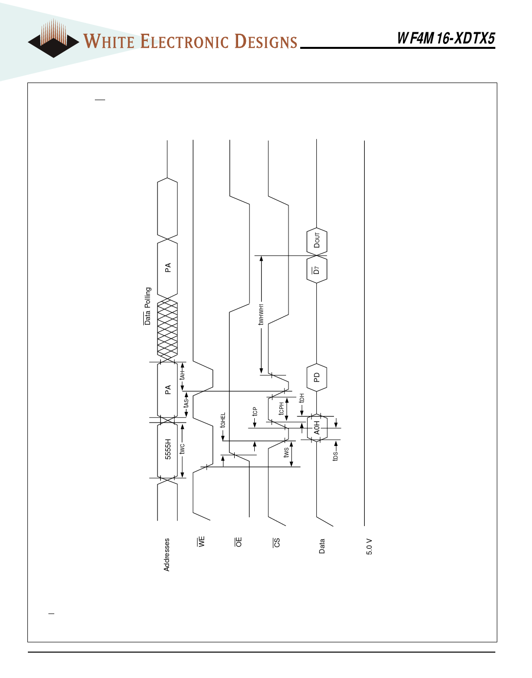
FIG. 7
ALTERNATE CS CONTROLLED
PROGRAMMING OPERATION TIMINGS
WF4M16-XDTX5
NOTES:
1. PA represents the address of the memory location to be programmed.
2. PD represents the data to be programmed at byte address.
3. D7 is the output of the complement of the data written to each chip.
4. DOUT is the output of the data written to the device.
5. Figure indicates the last two bus cycles of a four bus cycle sequence.
9
White Electronic Designs Corporation • (602) 437-1520 • www.whiteedc.com
Share Link: 