ADG1207 查看數據表(PDF) - Analog Devices
零件编号
产品描述 (功能)
生产厂家
ADG1207 Datasheet PDF : 20 Pages
| |||
Data Sheet
Low Capacitance, 16- and 8-Channel,
±15 V/+12 V iCMOS Multiplexers
ADG1206/ADG1207
FEATURES
<1 pC charge injection over full signal range
1.5 pF off capacitance
33 V supply range
120 Ω on resistance
Fully specified at ±15 V/+12 V
3 V logic-compatible inputs
Rail-to-rail operation
Break-before-make switching action
28-lead TSSOP and 32-lead, 5 mm × 5 mm LFCSP
APPLICATIONS
Audio and video routing
Automatic test equipment
Data acquisition systems
Battery-powered systems
Sample-and-hold systems
Communication systems
GENERAL DESCRIPTION
The ADG1206 and ADG1207 are monolithic iCMOS® analog
multiplexers comprising sixteen single channels and eight
differential channels, respectively. The ADG1206 switches one
of sixteen inputs to a common output, as determined by the
4-bit binary address lines A0, A1, A2, and A3. The ADG1207
switches one of eight differential inputs to a common differential
output, as determined by the 3-bit binary address lines A0, A1,
and A2. An EN input on both devices is used to enable or disable
the device. When disabled, all channels are switched off. When
on, each channel conducts equally well in both directions and
has an input signal range that extends to the supplies.
The industrial CMOS (iCMOS) modular manufacturing
process combines high voltage, complementary metal-oxide
semiconductor (CMOS) and bipolar technologies. It enables the
development of a wide range of high performance analog ICs
capable of 33 V operation in a footprint that no other generation
of high voltage devices has been able to achieve. Unlike analog
ICs using conventional CMOS processes, iCMOS components
can tolerate high supply voltages while providing increased
performance, dramatically lower power consumption, and
reduced package size.
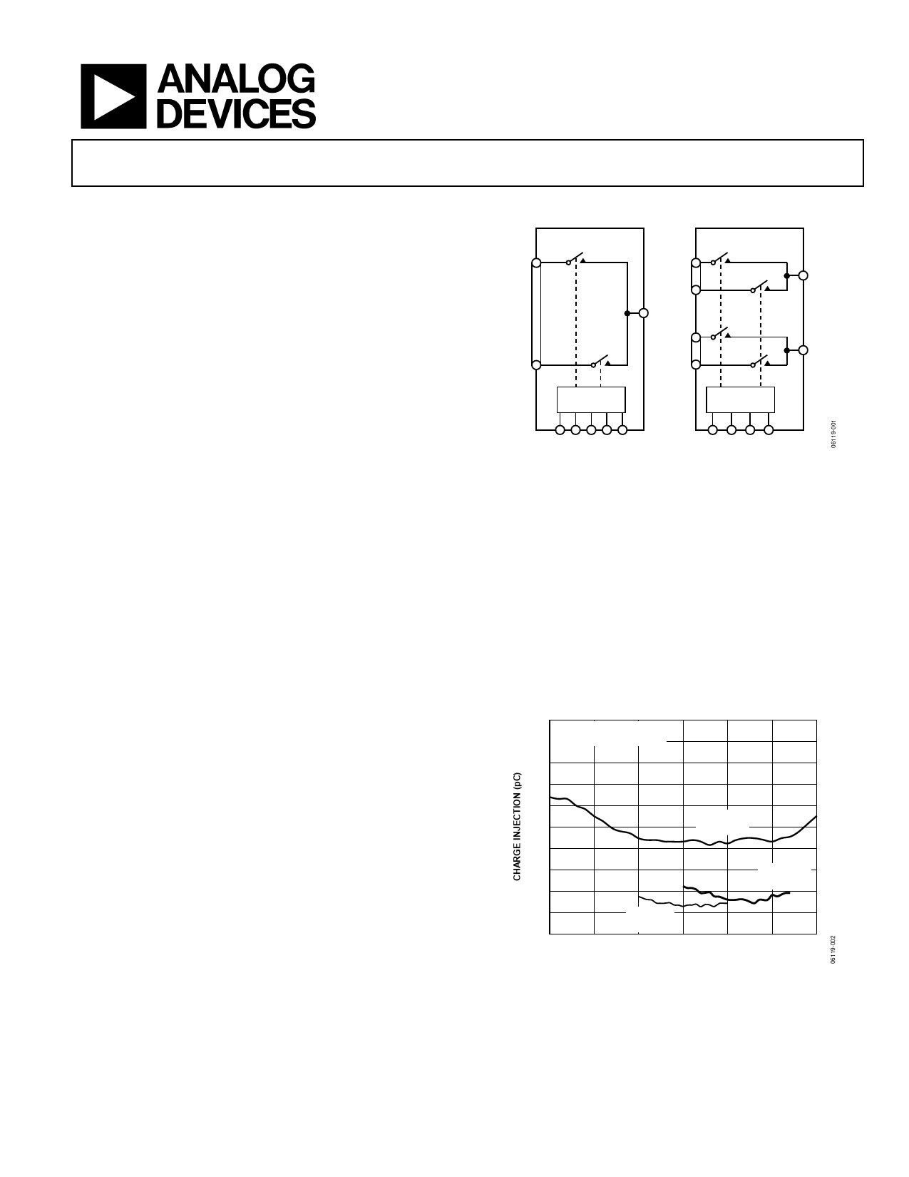
FUNCTIONAL BLOCK DIAGRAMS
ADG1206
S1
ADG1207
S1A
DA
S8A
D
S1B
DB
S16
S8B
1-OF-16
DECODER
1-OF-8
DECODER
A0 A1 A2 A3 EN
A0 A1 A2 EN
Figure 1.
The ultralow capacitance and exceptionally low charge injection
of these multiplexers make them ideal solutions for data acquisition
and sample-and-hold applications, where low glitch and fast
settling are required. Figure 2 shows that there is minimum
charge injection over the entire signal range of the device.
iCMOS construction also ensures ultralow power dissipation,
making the devices ideally suited for portable and battery-
powered instruments.
1.0
MUX (SOURCE TO DRAIN)
0.9 TA = 25°C
0.8
0.7
0.6
VDD = +15V
0.5
VSS = –15V
0.4
0.3
VDD = +12V
VSS = 0V
0.2
0.1
VDD = +5V
0
VSS = –5V
–15
–10
–5
0
5
10
15
VS (V)
Figure 2. Source-to-Drain Charge Injection vs. Source Voltage
Rev. C
Document Feedback
Information furnished by Analog Devices is believed to be accurate and reliable. However, no
responsibility is assumed by Analog Devices for its use, nor for any infringements of patents or other
rights of third parties that may result from its use. Specifications subject to change without notice. No
license is granted by implication or otherwise under any patent or patent rights of Analog Devices.
Trademarks and registered trademarks are the property of their respective owners.
One Technology Way, P.O. Box 9106, Norwood, MA 02062-9106, U.S.A.
Tel: 781.329.4700 ©2006–2016 Analog Devices, Inc. All rights reserved.
Technical Support
www.analog.com
Share Link: 