CXD2450R 查看數據表(PDF) - Sony Semiconductor
零件编号
产品描述 (功能)
生产厂家
CXD2450R Datasheet PDF : 30 Pages
| |||
CXD2450R
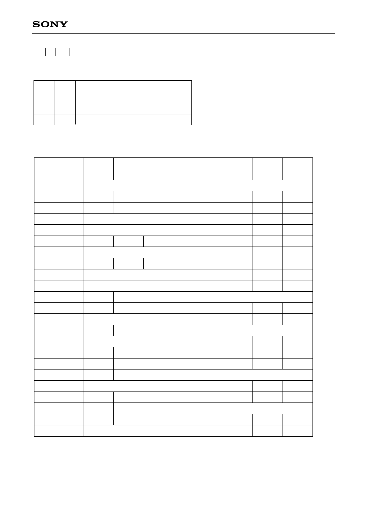
D62 to D63 STB
This switches the operating mode as shown below. However, the IC pin status control bit is loaded to the
CXD2450R and controlled immediately at the rise of the SEN input.
D63 D62
Symbol
Operating mode
X
0 CAMERA
Normal operating mode
0
1 SLEEP
Sleep mode∗1
1
1 STNBY
Standby mode
∗1 Mode for the status which does not require CCD drive when playing back recorded data within the system.
The pin status during each mode is shown in the table below.
Pin Symbol CAMERA SLEEP
1 3MCK
ACT
ACT
2 Vss1
—
3 WEN
ACT
L
4 ID
ACT
L
5 TEST
—
6 VDD1
—
7 XCLPOB ACT
L
8 VDD2
—
9 RG
ACT
L
10 Vss2
—
11 Vss3
—
12 H1
ACT
L
13 H2
ACT
L
14 VDD3
—
15 XCLPDM ACT
L
16 VDD4
—
17 XSHP
ACT
L
18 XSHD
ACT
L
19 XRS
ACT
L
20 Vss4
—
21 PBLK
ACT
L
22 1/2MCK
ACT
L
23 3/2MCK
ACT
ACT
24 VDD5
—
STNBY
ACT
L
L
L
L
L
L
L
L
L
L
L
L
L
Pin Symbol CAMERA SLEEP
25 RST
ACT
ACT
26 VDD6
—
27 SSI
ACT
ACT
28 SSK
ACT
ACT
29 SEN
ACT
ACT
30 EBCKSM ACT
ACT
31 FRO
ACT
ACT
32 HRO
ACT
ACT
33 HRI
ACT
ACT
34 FRI
ACT
ACT
35 CLD
ACT
L
36 Vss5
—
37 DSGAT
ACT
ACT
38 MCK
ACT
ACT
39 VM
—
40 V1
ACT
VM
41 V3
ACT
VM
42 V2a
ACT
VH
43 VH
—
44 V2b
ACT
VH
45 VSUB
ACT
VH
46 VL
—
47 OSCO
ACT
ACT
48 OSCI
ACT
ACT
STNBY
ACT
ACT
ACT
ACT
ACT
L
L
ACT
ACT
L
ACT
L
VM
VM
VH
VH
VH
ACT
ACT
Note) ACT means that the circuit is operating. L indicates a low output level in the controlled status.
Also, VH and VM indicate the voltage levels applied to VH (Pin 43) and VM (Pin 39), respectively, in
the control status.
– 20 –
Share Link: 