STB85NF3LL-1 Просмотр технического описания (PDF) - STMicroelectronics
Номер в каталоге
Компоненты Описание
производитель
STB85NF3LL-1
STMicroelectronics
STB85NF3LL-1 Datasheet PDF : 9 Pages
| |||
STP85NF3LL/STB85NF3LL-1
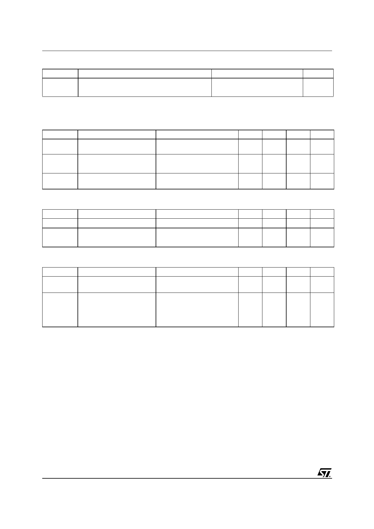
THERMAL DATA
Rthj-case Thermal Resistance Junction-case Max
1.36
Rthj-amb Thermal Resistance Junction-ambient Max
62.5
Tl
Maximum Lead Temperature For Soldering Purpose
300
°C/W
°C/W
°C
ELECTRICAL CHARACTERISTICS (TCASE = 25 °C UNLESS OTHERWISE SPECIFIED)
OFF
Symbol
Parameter
Test Conditions
Min. Typ. Max. Unit
V(BR)DSS Drain-source
ID = 250 µA, VGS = 0
30
V
Breakdown Voltage
IDSS
Zero Gate Voltage
Drain Current (VGS = 0)
VDS = Max Rating
VDS = Max Rating, TC = 125 °C
1
µA
10
µA
IGSS
Gate-body Leakage
Current (VDS = 0)
VGS = ± 15V
±100
nA
ON (1)
Symbol
VGS(th)
RDS(on)
Parameter
Gate Threshold Voltage
Static Drain-source On
Resistance
Test Conditions
VDS = VGS, ID = 250µA
VGS = 10V, ID = 40 A
VGS = 4.5V, ID = 40 A
Min.
1
Typ. Max.
0.006 0.008
0.0075 0.0095
Unit
V
Ω
Ω
DYNAMIC
Symbol
gfs (1)
Parameter
Forward Transconductance
Ciss
Coss
Crss
Input Capacitance
Output Capacitance
Reverse Transfer
Capacitance
Test Conditions
VDS > ID(on) x RDS(on)max,
ID = 40 A
VDS = 25V, f = 1 MHz, VGS = 0
Min.
Typ.
30
2210
635
138
Max.
Unit
S
pF
pF
pF
2/9
Share Link: 