ZXLD1356QET5TA(2012) Просмотр технического описания (PDF) - Diodes Incorporated.
Номер в каталоге
Компоненты Описание
производитель
ZXLD1356QET5TA Datasheet PDF : 29 Pages
| |||
A Product Line of
Diodes Incorporated
ZXLD1356/ ZXLD1356Q
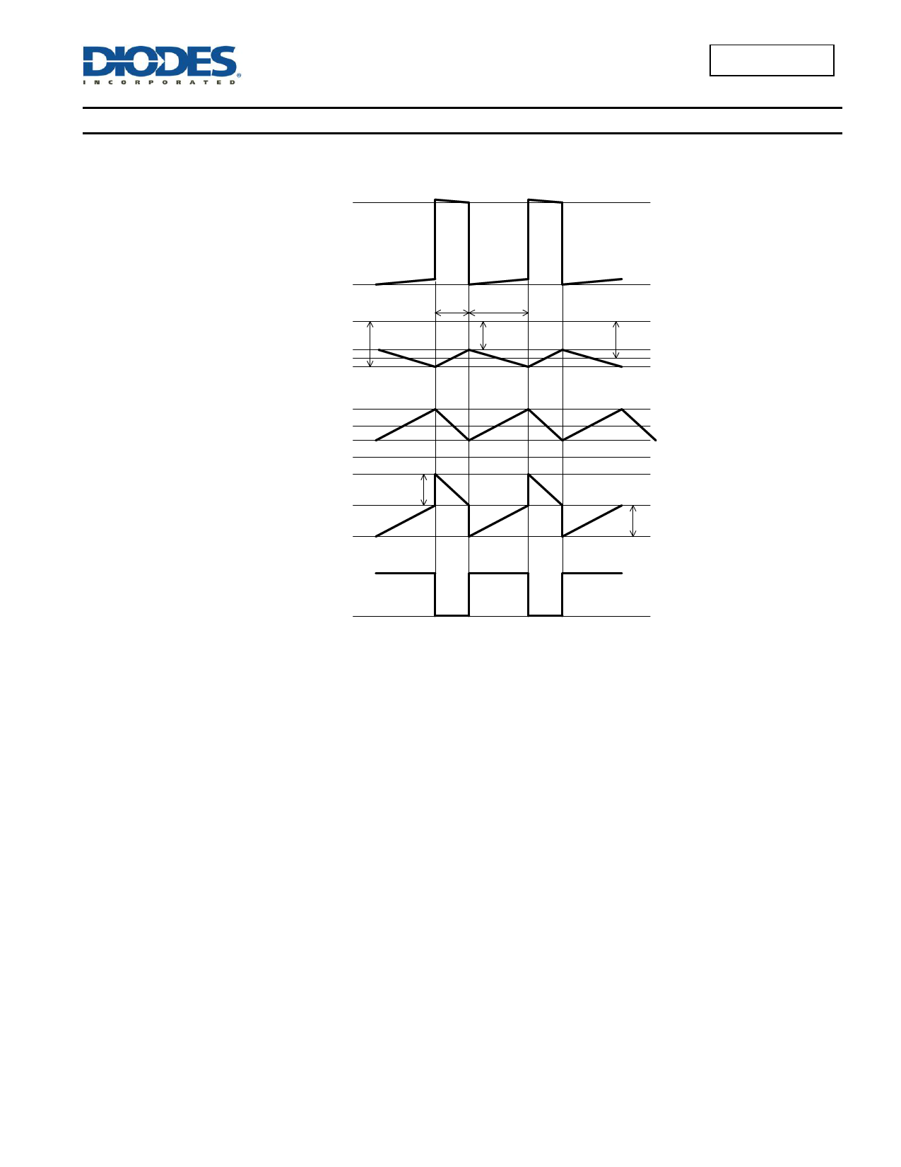
Electrical Characteristics (VIN = 24V, @TAMB = +25°C, unless otherwise specified.)
Symbol
Parameter
Condition
Min
Typ
Max Unit
VSU
VSD
IINQoff
IINQon
Internal regulator start-up threshold
Internal regulator shutdown threshold
Quiescent supply current with output off
Quiescent supply current with output switching
(Note 6)
ADJ pin grounded
ADJ pin floating, L = 68mH,
3 LEDsf = 360kHz
4.85
5.2
V
4.40 4.75
V
65
108 µA
1.6
mA
VSENSE
VSENSEHYS
ISENSE
VREF
Mean current sense threshold voltage
(Defines LED current setting accuracy)
Sense threshold hysteresis
ISENSE pin input current
Internal reference voltage
Measured on ISENSE pin with respect
195
to VIN VADJ = 1.25V; VIN = 18V
VSENSE = VIN -0.2
Measured on ADJ pin with pin
floating
200
±15
4
1.25
205 mV
%
10
µA
V
ΔVREF/ΔT
VADJ
VADJoff
VADJon
RADJ
Temperature coefficient of VREF
External control voltage range on ADJ pin for
DC brightness control (Note 7)
DC voltage on ADJ pin to switch device from
active (on) state to quiescent (off) state
DC voltage on ADJ pin to switch device from
quiescent (off) state to active (on) state
Resistance between ADJ pin and VREF
0.3
VADJ falling
0.15
VADJ rising
0< VADJ < VREF, VADJ > VREF +100mV
0.2
30
10.4
50
0.20
0.25
50
14.2
ppm/°C
2.5
V
0.27
V
0.3
V
65
18.0
kΩ
ILXmean
Continuous LX switch current
0.55
A
RLX
LX switch ‘On’ resistance
@ ILX = 0.55A
0.5
0.75 Ω
ILX(leak)
LX switch leakage current
5
µA
DPWM(LF)
Duty cycle range of PWM signal applied to ADJ
pin during low frequency PWM dimming mode
Brightness control range
PWM frequency <300Hz PWM
amplitude = VREF
Measured on ADJ pin
0.001
1
1000:1
DCADJ(*)
DC Brightness control range
Note 8
5:1
Start up time
tSS
(See graphs for more details)
Time taken for output current to reach
90% of final value after voltage on
ADJ pin has risen above 0.3V.
2
ms
Requires external capacitor 22nF.
Operating frequency
fLX
(See graphs for more details)
ADJ pin floating L= 68mH (0.36V)
IOUT = 0.55A @ VLED = 3.6V
Driving 3 LEDs
360
kHz
fLXmax
Recommended maximum operating frequency
500 kHz
Notes:
6. Static current of device is approximately 700 µA, see Graph, Page 17.
7. 100% brightness corresponds to VADJ = VADJ(nom) = VREF. Driving the ADJ pin above VREF will increase the VSENSE. threshold and output current
proportionally.
8. Ratio of maximum brightness to minimum brightness before shutdown VREF =1.25/0.25. VREF externally driven to 2.5V, ratio 10.1.
ZXLD1356/ ZXLD1356Q
Document number: DS33470 Rev. 4 - 2
5 of 29
www.diodes.com
October 2012
© Diodes Incorporated
Share Link: 