74LVC126A-Q100 Просмотр технического описания (PDF) - Nexperia B.V. All rights reserved
Номер в каталоге
Компоненты Описание
производитель
74LVC126A-Q100
Nexperia B.V. All rights reserved
74LVC126A-Q100 Datasheet PDF : 13 Pages
| |||
Nexperia
4. Functional diagram
74LVC126A-Q100
Quad buffer/line driver with 5 V tolerant input/outputs; 3-state
2 1A
1 1OE
5 2A
4 2OE
9 3A
1Y 3
2Y 6
3Y 8
10 3OE
12 4A
13 4OE
4Y 11
Fig. 1. Logic symbol
mna235
nA
2
1
3
1
EN1
5
6
4
9
8
10
12
11
13
mna236
Fig. 2. IEC logic symbol
nY
nOE
Fig. 3. Logic diagram
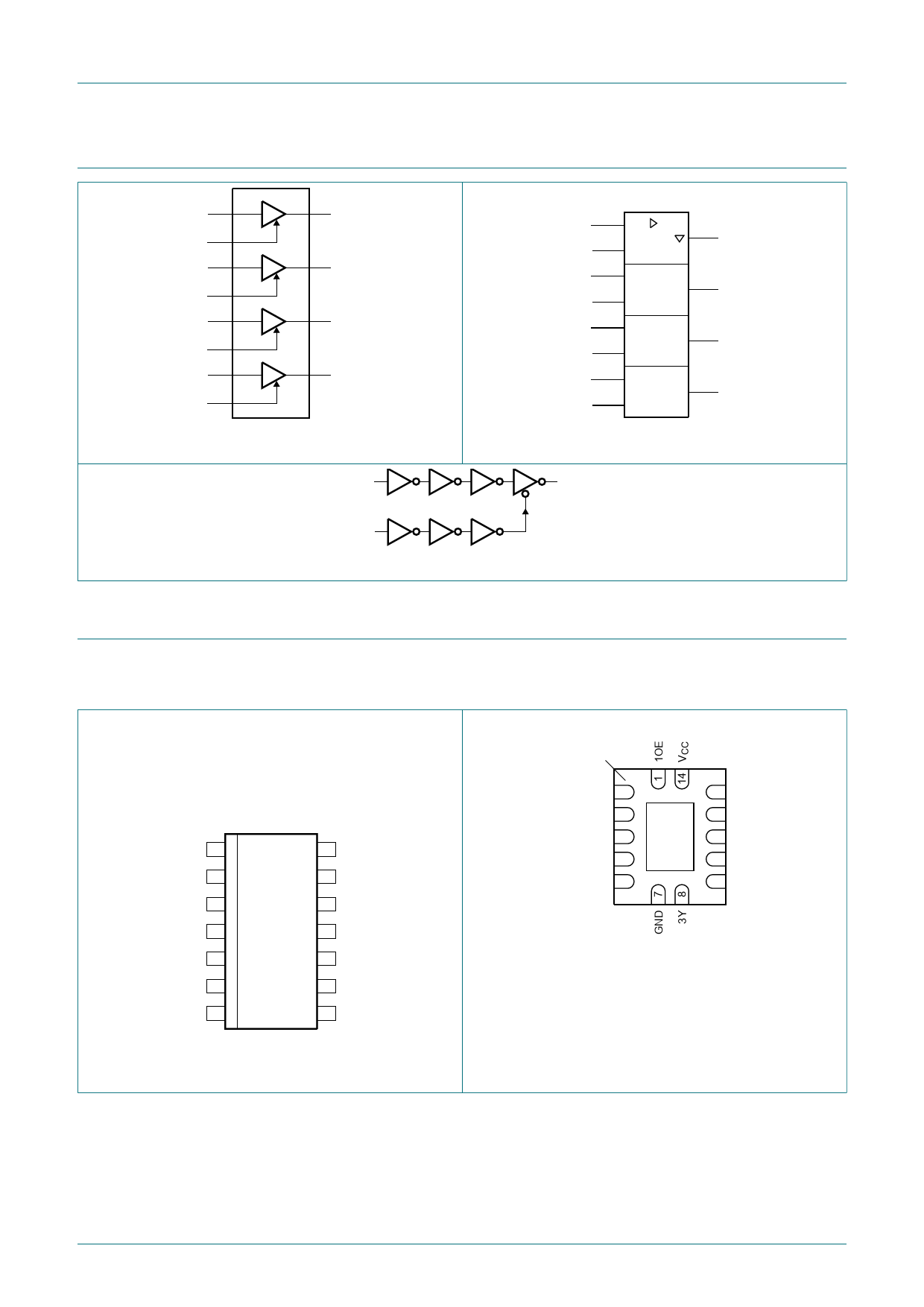
5. Pinning information
mna234
5.1. Pinning
74LVC126A-Q100
1OE 1
14 VCC
1A 2
13 4OE
1Y 3
12 4A
2OE 4
11 4Y
2A 5
10 3OE
2Y 6
9 3A
GND 7
8 3Y
aaa-012464
Fig. 4. Pin configuration SOT108-1 (SO14) and
SOT402-1 (TSSOP14)
74LVC126A-Q100
terminal 1
index area
1A 2
1Y 3
2OE 4
2A 5
2Y 6
GND(1)
13 4OE
12 4A
11 4Y
10 3OE
9 3A
aaa-012465
Transparent top view
(1) This is not a supply pin. The substrate is
attached to this pad using conductive die attach
material. There is no electrical or mechanical
requirement to solder this pad. However, if it is
soldered, the solder land should remain floating or
be connected to GND.
Fig. 5. Pin configuration SOT762-1 (DHVQFN14)
74LVC126A_Q100
Product data sheet
All information provided in this document is subject to legal disclaimers.
Rev. 2 — 21 August 2018
© Nexperia B.V. 2018. All rights reserved
2 / 13
Share Link: 