HIP6006 Просмотр технического описания (PDF) - Renesas Electronics
Номер в каталоге
Компоненты Описание
производитель
HIP6006 Datasheet PDF : 12 Pages
| |||
HIP6006
PUPPER = IO2 x rDS(ON) x D +
1
2
Io x VIN x tSW x Fs
PLOWER = IO2 x rDS(ON) x (1 - D)
Where: D is the duty cycle = VO / VIN,
tSW is the switching interval, and
Fs is the switching frequency.
tSW which increases the upper MOSFET switching losses.
Ensure that both MOSFETs are within their maximum junction
temperature at high ambient temperature by calculating the
temperature rise according to package thermal-resistance
specifications. A separate heatsink may be necessary
depending upon MOSFET power, package type, ambient
temperature and air flow.
Standard-gate MOSFETs are normally recommended for use
with the HIP6006. However, logic-level gate MOSFETs can be
used under special circumstances. The input voltage, upper
gate drive level, and the MOSFETs absolute gate-to-source
voltage rating determine whether logic-level MOSFETs are
appropriate.
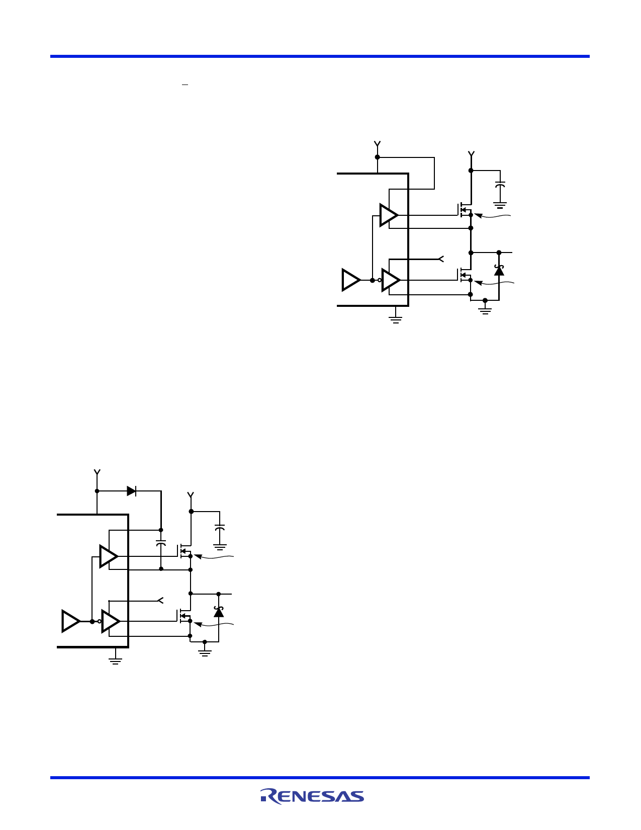
Figure 9 shows the upper gate drive (BOOT pin) supplied by a
bootstrap circuit from VCC. The boot capacitor, CBOOT
develops a floating supply voltage referenced to the PHASE
pin. This supply is refreshed each cycle to a voltage of VCC
less the boot diode drop (VD) when the lower MOSFET, Q2
turns on. A logic-level MOSFET can only be used for Q1 if the
MOSFETs absolute gate-to-source voltage rating exceeds the
maximum voltage applied to VCC. For Q2, a logic-level
MOSFET can be used if its absolute gate-to-source voltage
rating exceeds the maximum voltage applied to PVCC.
+12V
DBOOT
VCC
+-
VD
+5V OR +12V
HIP6006
BOOT
UGATE
PHASE
CBOOT
Q1
NOTE:
VG-S VCC - VD
+5V
PVCC OR +12V
-
+
LGATE
PGND
Q2
D2
NOTE:
VG-S PVCC
GND
FIGURE 9. UPPER GATE DRIVE - BOOTSTRAP OPTION
VCC less the input supply. For +5V main power and +12 VDC
for the bias, the gate-to-source voltage of Q1 is 7V. A logic-
level MOSFET is a good choice for Q1 and a logic-level
MOSFET can be used for Q2 if its absolute gate-to-source
voltage rating exceeds the maximum voltage applied to PVCC.
+12V
VCC
HIP6006
-
+
+5V OR LESS
BOOT
Q1
UGATE
PHASE
+5V
PVCC OR +12V
Q2
LGATE
PGND
NOTE:
VG-S VCC - 5V
D2
NOTE:
VG-S PVCC
GND
FIGURE 10. UPPER GATE DRIVE - DIRECT VCC DRIVE OPTION
Schottky Selection
Rectifier D2 is a clamp that catches the negative inductor swing
during the dead time between turning off the lower MOSFET
and turning on the upper MOSFET. The diode must be a
Schottky type to prevent the lossy parasitic MOSFET body diode
from conducting. It is acceptable to omit the diode and let the
body diode of the lower MOSFET clamp the negative inductor
swing, but efficiency will drop one or two percent as a result. The
diode's rated reverse breakdown voltage must be greater than
the maximum input voltage.
Figure 10 shows the upper gate drive supplied by a direct
connection to VCC. This option should only be used in
converter systems where the main input voltage is +5 VDC or
less. The peak upper gate-to-source voltage is approximately
FN4306 Rev.3.00
April 1, 2005
Page 9 of 12
Share Link: 