HIP6501AEVAL1 Просмотр технического описания (PDF) - Renesas Electronics
Номер в каталоге
Компоненты Описание
производитель
HIP6501AEVAL1 Datasheet PDF : 14 Pages
| |||
HIP6501A
Soft-Start into Active States (S0, S1)
If both S3 and S5 are logic high at the time the 5VSB is
applied, the HIP6501A will assume an active state and keep
off the controlled external transistors until about 50ms after
the ATX’s 12V output (sensed at the 12V pin) exceeds the
set threshold (typically 10.8V). This timeout feature is
necessary in order to ensure the main ATX outputs are
stabilized. The timeout also assures smooth transitions from
sleep into active when sleep states are being supported.
During sleep to active state transitions from conditions
where the outputs are initially 0V (such as S4/S5 to S0
transition with EN3VDL = 1 and EN5VDL = 0, or simple
power-up sequence directly into active state), the 3VDUAL
and 5VDUAL outputs go through a quasi soft-start by being
pulled high through the body diodes of the N-channel
MOSFETs connected between these outputs and the 3.3V
and 5V ATX outputs, respectively. Figure 10 shows this start-
up scenario.
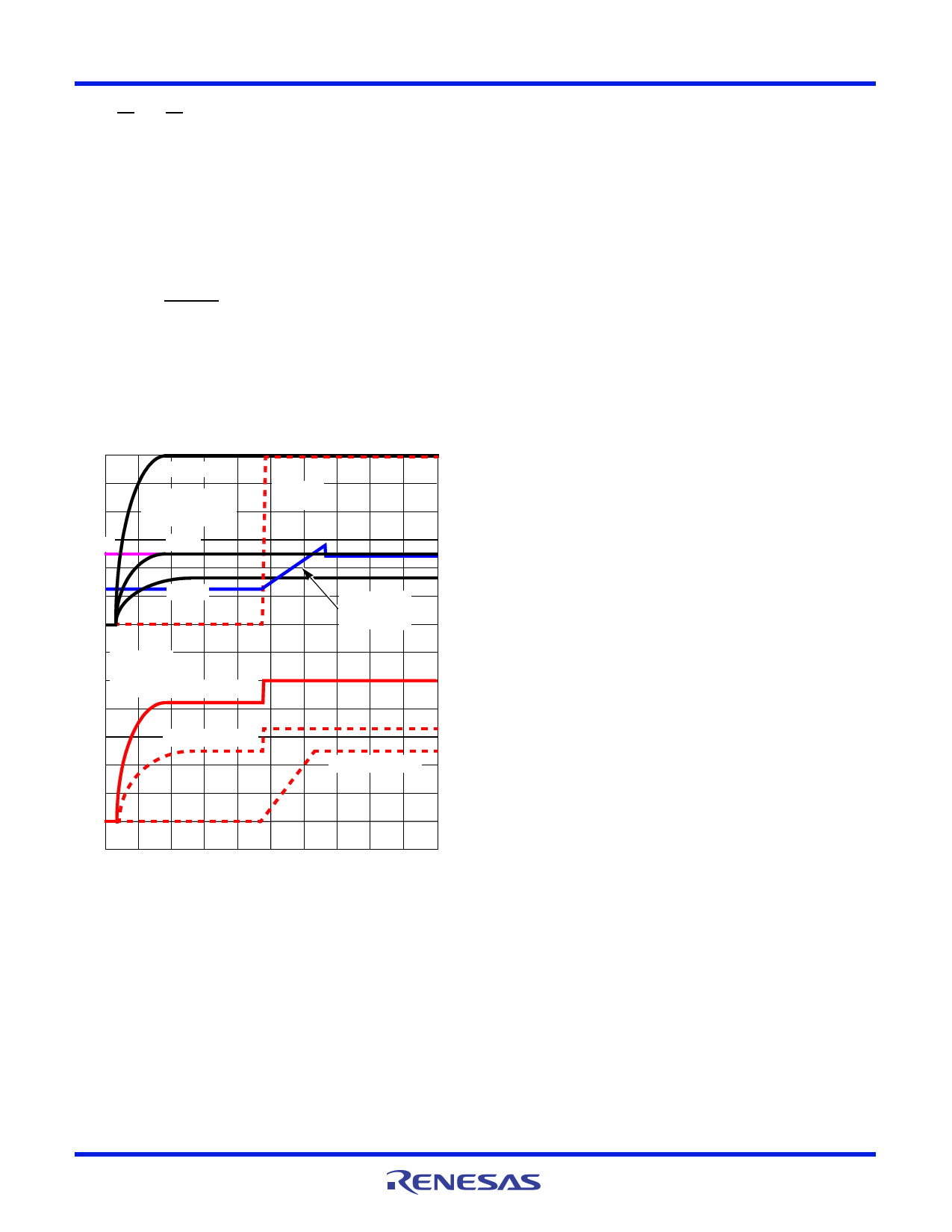
+5VSB
+12VIN
INPUT VOLTAGES
(2V/DIV)
+5VIN
DLA PIN
(2V/DIV)
+3.3VIN
0V
OUTPUT
VOLTAGES
(1V/DIV) VOUT3 (5VDUAL)
SOFT-START
(1V/DIV)
VOUT1 (3.3VDUAL)
VOUT2 (2.5VMEM)
0V
T0 T1
T2
T3 T4
TIME
FIGURE 10. SOFT-START INTERVAL IN AN ACTIVE STATE
5VSB is already present when the main ATX outputs are
turned on at time T0. Similarly, the soft-start capacitor has
already been charged up to 1.25V and the clamp is active,
awaiting for the 12V POR timer to expire. As a result of
3.3VIN and 5VIN ramping up, the 3.3VDUAL and 5VDUAL
output capacitors charge up through the body diodes of Q3
and Q5, respectively (see Figure 3). At time T1, the 12V ATX
output exceeds the HIP6501A’s 12V under-voltage
threshold, and the internal 50ms (typical) timer is initiated. At
T2 the time-out initiates a soft-start, and the memory output
is ramped-up, reaching regulation limits at time T3.
FN4749 Rev 6.00
December 30, 2004
Simultaneous with the memory voltage ramp-up, the DLA
pin is pulled high (to 12V), turning on Q3 and Q5, and
bringing the 3.3VDUAL and 5VDUAL outputs in regulation at
time T2. At time T4, when the soft-start voltage reaches
approximately 2.8V, the under-voltage monitoring circuits are
enabled and the soft-start capacitor is quickly discharged to
approximately 2.45V.
Requests to go into a sleep state during an active state soft-
start ramp-up result in a chip reset, followed by a new soft-
start sequence into the desired state.
Fault Protection
All the outputs are monitored against under-voltage events.
A severe over-current caused by a failed load on any of the
outputs, would, in turn, cause that specific output to
suddenly drop. If any of the output voltages drop below 69%
of their set value, such event is reported by having the
FAULT/MSEL pin pulled to 5V. Additionally, the 2.5/3.3V
memory regulator is internally current limited while in a sleep
state. Exceeding the maximum current rating of this output in
a sleep state can lead to output voltage drooping. If
excessive, this droop can ultimately trip the under-voltage
detector and send a FAULT signal to the computer system.
However, a FAULT condition will only set off the FAULT flag,
and it will not shut off or latch off any part of the circuit. If
shutdown or latch off of the circuit is desired, this can be
achieved by externally pulling or latching the SS pin low.
Pulling the SS pin low will also force the FAULT pin to go low.
Under-voltage sensing is disabled on all disabled outputs
and during soft-start ramp-up intervals. SS voltage reaching
the 2.8V threshold signals activation of the under-voltage
monitor.
Another condition that could set off the FAULT flag is chip
over-temperature. If the HIP6501A reaches an internal
temperature of 125oC (minimum), the FAULT flag is set
(FAULT/MSEL pulled high), but the chip continues to operate
until the temperature reaches 150oC (typical), when
unconditional latched shutdown of all outputs takes place.
The thermal latch can be reset only by cycling the 5VSB off,
and then on.
Output Voltages
The output voltages are internally set and do not require any
external components. Selection of the memory voltage is
done by means of an external resistor connected between
the FAULT/MSEL pin and ground. An internal 40A (typical)
current source creates a voltage drop across this resistor.
During every 5VSB trip above POR level, this voltage is
compared with an internal reference (200mV typically).
Based on this comparison, the output voltage is set at either
2.5V (RSEL = 1k), or 3.3V (RSEL = 10k). It is very
important that no capacitor is connected to the FAULT/MSEL
pin; the presence of a capacitive element at this pin can lead
to false memory voltage selection. See Figure 11 for details.
Page 9 of 14
Share Link: 