IR51H320 Просмотр технического описания (PDF) - International Rectifier
Номер в каталоге
Компоненты Описание
производитель
IR51H320 Datasheet PDF : 7 Pages
| |||
IR51H(D)224
IR51H(D)320
IR51H(D)420
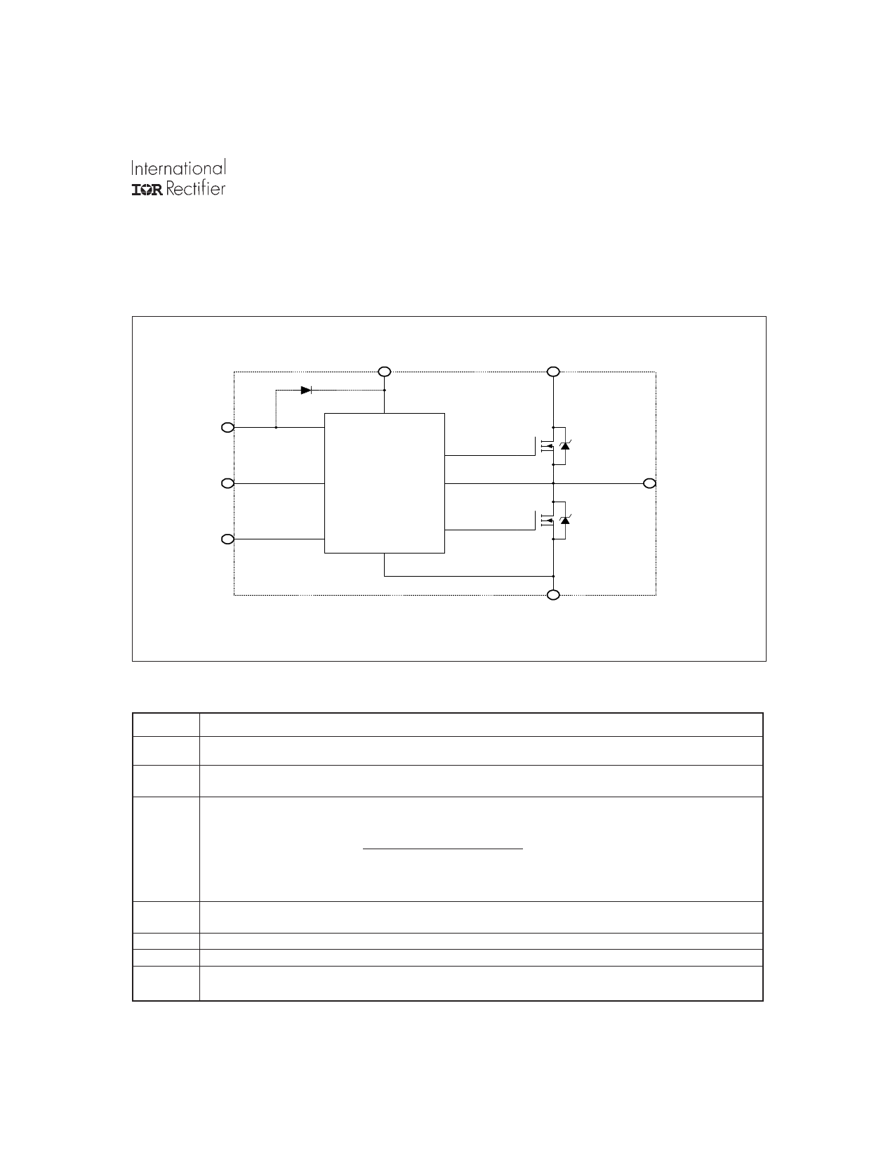
Functional Block Diagram
VB
D1
6
1
Vcc
2
RT
3
CT
HO
IR2151
VS
LO
Fast recovery diode D1 is
incorporated in IR51HDXXX only
VIN
9
IRFCXXX
7
VO
IRFCXXX
4
COM
Lead Definitions
Symbol
VCC
RT
CT
VB
VIN
VO
COM
Lead Description
Logic and internal gate drive supply voltage. An internal zener clamp diode at 15.6 V norminal is included
to allow the VCC to be current fed directly from VIN typically by means of a high value resistor.
Oscillator timing resistor output; a resistor is connected from RT to CT. RT is out of phase with the half-
bridge output (VO).
Oscillator timing capacitor input; a capacitor is connected from CT to COM in order to program the
oscillator frequency according to the following equation:
f=
1
1. 4 × (RT + 75Ω) × CT
CT PIN also invokes shutdown function (see note 2) where 75Ω is the effective impedence of the RT
output stage.
High side gate drive floating supply. For bootstrap operation a high voltage fast recovery diode is needed
to feed from VCC to VB. (HD type circuits incorporate this diode).
High voltage supply
Half Bridge output
Logic and low side of half bridge return
5
Share Link: 