FDC6331L Просмотр технического описания (PDF) - Fairchild Semiconductor
Номер в каталоге
Компоненты Описание
производитель
FDC6331L Datasheet PDF : 4 Pages
| |||
0.4
0.35
0.3
VIN = 1.8V
VON/OFF = 1.5V -8V
PW = 300us, D < 2%
0.25
T J = 125OC
0.2
0.15
TJ = 25 OC
0.1
0.05
0
0
1
2
3
4
5
6
IL, (A)
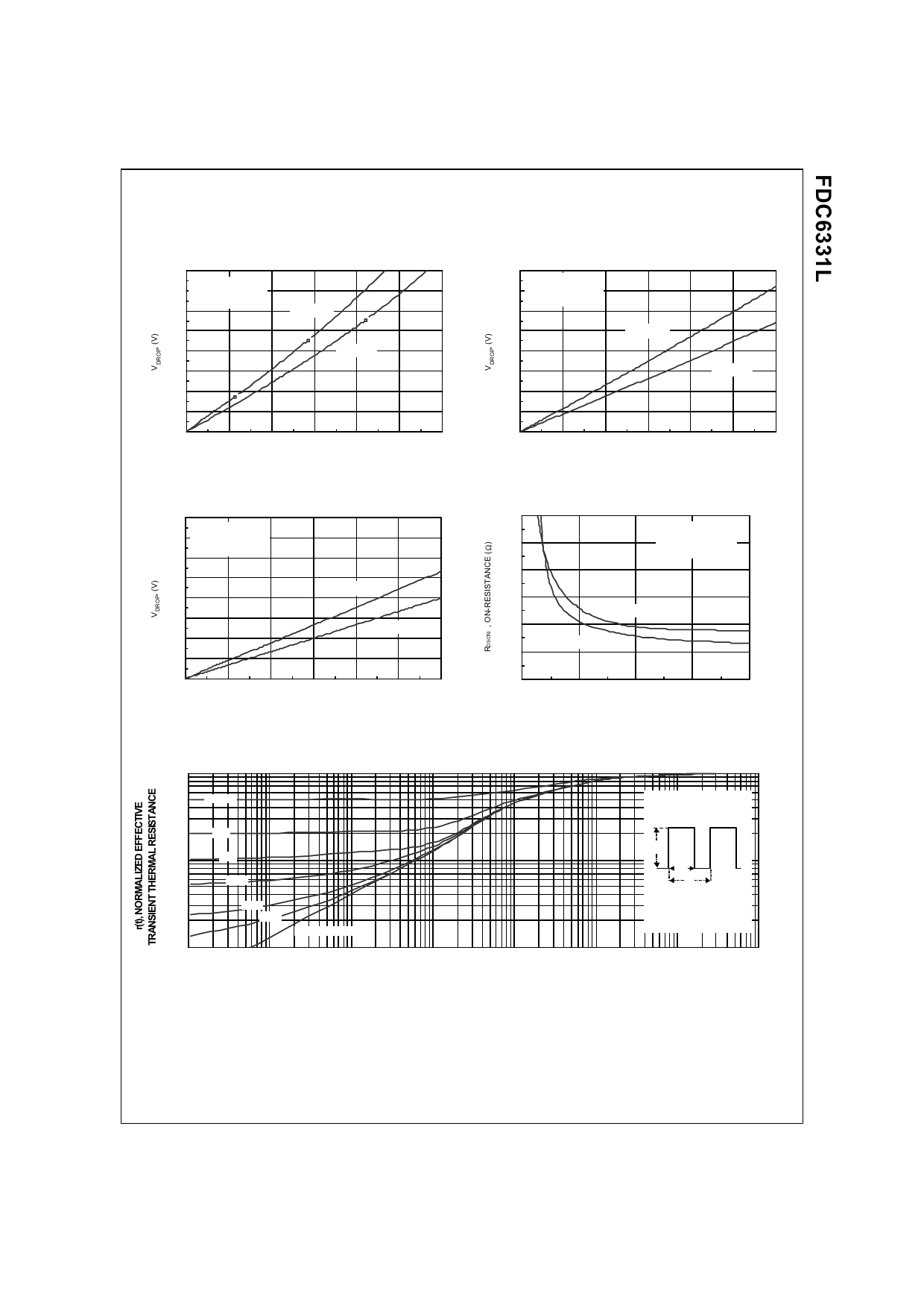
Figure 1. Conduction Voltage Drop
Variation with Load Current.
0.4
0.35
0.3
VIN = 4.5V
VON/OFF = 1.5V -8V
PW = 300us, D < 2%
0.25
0.2
TJ = 125 OC
0.15
0.1
TJ = 25OC
0.05
0
0
1
2
3
4
5
6
IL, (A)
Figure 3. Conduction Voltage Drop
Variation with Load Current.
0.4
0.35
0.3
VIN = 2.5V
VON/OFF = 1.5V -8V
PW = 300us, D < 2%
0.25
0.2
0.15
TJ = 125 OC
T J = 25OC
0.1
0.05
0
0
1
2
3
4
5
6
IL, (A)
Figure 2. Conduction Voltage Drop
Variation with Load Current.
0.15
0.125
Q2
IL = 1A
VON/OFF = 1.5V -8V
PW = 300us, D < 2%
0.1
0.075
0.05
0.025
T J = 125OC
TJ = 25OC
0
1
2
3
4
5
-VGS , GATE TO SOURCE VOLTAGE (V)
Figure 4. On-Resistance Variation
With Input Voltage
1
D = 0.5
RTJA(t) = r(t) + RTJA
RTJA = 156 °C/W
0.2
0.1
0.1
0.05
0.02
0.01
SINGLE PULSE
P(pk)
t1
t2
TJ - TA = P * RTJA(t)
Duty Cycle, D = t1/ t2
0.01
0.0001
0.001
0.01
0.1
1
10
100
1000
Figure 5. Transient Thermal Response Curve.
Thermal characterization performed on the conditions described in Note 2.
Transient thermal response will change depends on the circuit board design.
FDC6331L Rev D
Share Link: 