ISL6522ACB Просмотр технического описания (PDF) - Renesas Electronics
Номер в каталоге
Компоненты Описание
производитель
ISL6522ACB Datasheet PDF : 14 Pages
| |||
ISL6522A
Absolute Maximum Ratings
Supply Voltage, VCC . . . . . . . . . . . . . . . . . . . . . . . . . . . . . . . +15.0V
Boot Voltage, VBOOT - VPHASE . . . . . . . . . . . . . . . . . . . . . . +15.0V
Input, Output or I/O Voltage . . . . . . . . . . . . GND -0.3V to VCC +0.3V
ESD Classification . . . . . . . . . . . . . . . . . . . . . . . . . . . . . . . . . Class 2
Recommended Operating Conditions
Supply Voltage, VCC . . . . . . . . . . . . . . . . . . . . . . . . . . . +12V 10%
Ambient Temperature Range, ISL6522AC. . . . . . . . . . 25°C to 70°C
Junction Temperature Range, ISL6522AC . . . . . . . . . 0°C to 125°C
Thermal Information
Thermal Resistance
JA(°C/W) JC(°C/W)
QFN Package (Notes 1, 2). . . . . . . . . .
36
5
SOIC Package (Note 1) . . . . . . . . . . . .
65
N/A
Maximum Junction Temperature . . . . . . . . . . . . . . . . . . . . . . 150°C
Maximum Storage Temperature Range . . . . . . . . . . . -65°C to 150°C
Maximum Lead Temperature (Soldering 10s) . . . . . . . . . . . . 300°C
(SOIC - Lead Tips Only)
CAUTION: Stresses above those listed in “Absolute Maximum Ratings” may cause permanent damage to the device. This is a stress only rating and operation of the
device at these or any other conditions above those indicated in the operational sections of this specification is not implied.
NOTES:
1. JA is measured in free air with the component mounted on a high effective thermal conductivity test board with “direct attach” features. SeeTech
Brief TB379.
2. For JC, the "case temp" location is the center of the exposed metal pad on the package underside.
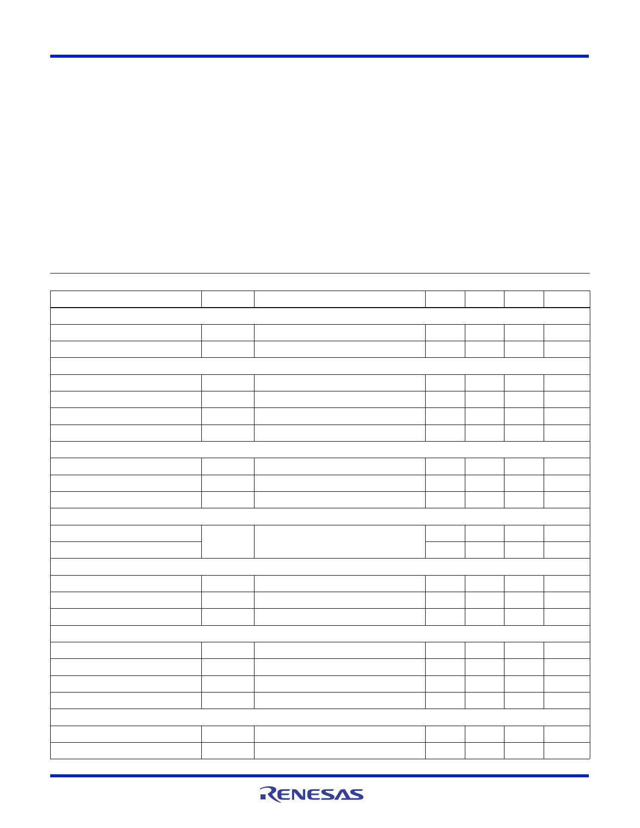
Electrical Specifications Recommended Operating Conditions, Unless Otherwise Noted
PARAMETER
SYMBOL
TEST CONDITIONS
MIN
TYP
MAX
UNITS
VCC SUPPLY CURRENT
Nominal Supply
Shutdown Supply
ICC
EN = VCC; UGATE and LGATE Open
EN = 0V
-
5
-
mA
-
50
100
A
POWER-ON RESET
Rising VCC Threshold
Falling VCC Threshold
Enable-Input Threshold Voltage
Rising VOCSET Threshold
OSCILLATOR
VOCSET = 4.5VDC
VOCSET = 4.5VDC
VOCSET = 4.5VDC
-
-
10.4
V
8.1
-
-
V
0.8
-
2.0
V
-
1.27
-
V
Free Running Frequency
Total Variation
Ramp Amplitude
REFERENCE
VOSC
RT = OPEN, VCC = 12
6k < RT to GND < 200k
RT = OPEN
175
200
230
kHz
-20
-
+20
%
-
1.9
-
VP-P
Reference Voltage Tolerance
Reference Voltage
VREF
-0.5
-
0.5
%
-
0.800
-
V
ERROR AMPLIFIER
DC Gain
-
88
-
dB
Gain-Bandwidth Product
GBW
-
15
-
MHz
Slew Rate
SR
COMP = 10pF
-
6
-
V/s
GATE DRIVERS
Upper Gate Source
Upper Gate Sink
Lower Gate Source
Lower Gate Sink
PROTECTION
IUGATE
RUGATE
ILGATE
RLGATE
VBOOT - VPHASE = 12V, VUGATE = 6V
ILGATE = 0.3A
VCC = 12V, VLGATE = 6V
ILGATE = 0.3A
350
500
-
mA
-
5.5
10
300
450
-
mA
-
3.5
6.5
OCSET Current Source
Soft-Start Current
IOCSET
ISS
VOCSET = 4.5VDC
170
200
230
A
-
10
-
A
FN9122 Rev 2.00
Apr 13, 2005
Page 4 of 14
Share Link: 