B320B Просмотр технического описания (PDF) - Diode Semiconductor Korea
Номер в каталоге
Компоненты Описание
производитель
B320B Datasheet PDF : 2 Pages
| |||
Diode Semiconductor Korea
B320B-B360B
SURFACE MOUNT SCHOTTKY
BARRIER RECTIFIERS
REVERSE VOLTAGE: 20 --- 60 V
CURRENT: 3.0 A
FEATURES
◇ Plastic package has Underwriters Laborator
111 Flammability Classification 94V-0
◇ For surface mounted applications
◇ Low profile package
◇ Built-in strain relief
◇ Metal silicon junction, majority carrier conduction
◇ High surge capability
◇ High current capability,low forward voltage drop
◇ Low power loss,high effciency
◇ For use in low voltage high frequency inverters,free
111 wheeling and polarity protection applications
◇ Guardring for overvoltage protection
◇ High temperature soldering guaranteed:250oC/10 1
11 seconds at terminals
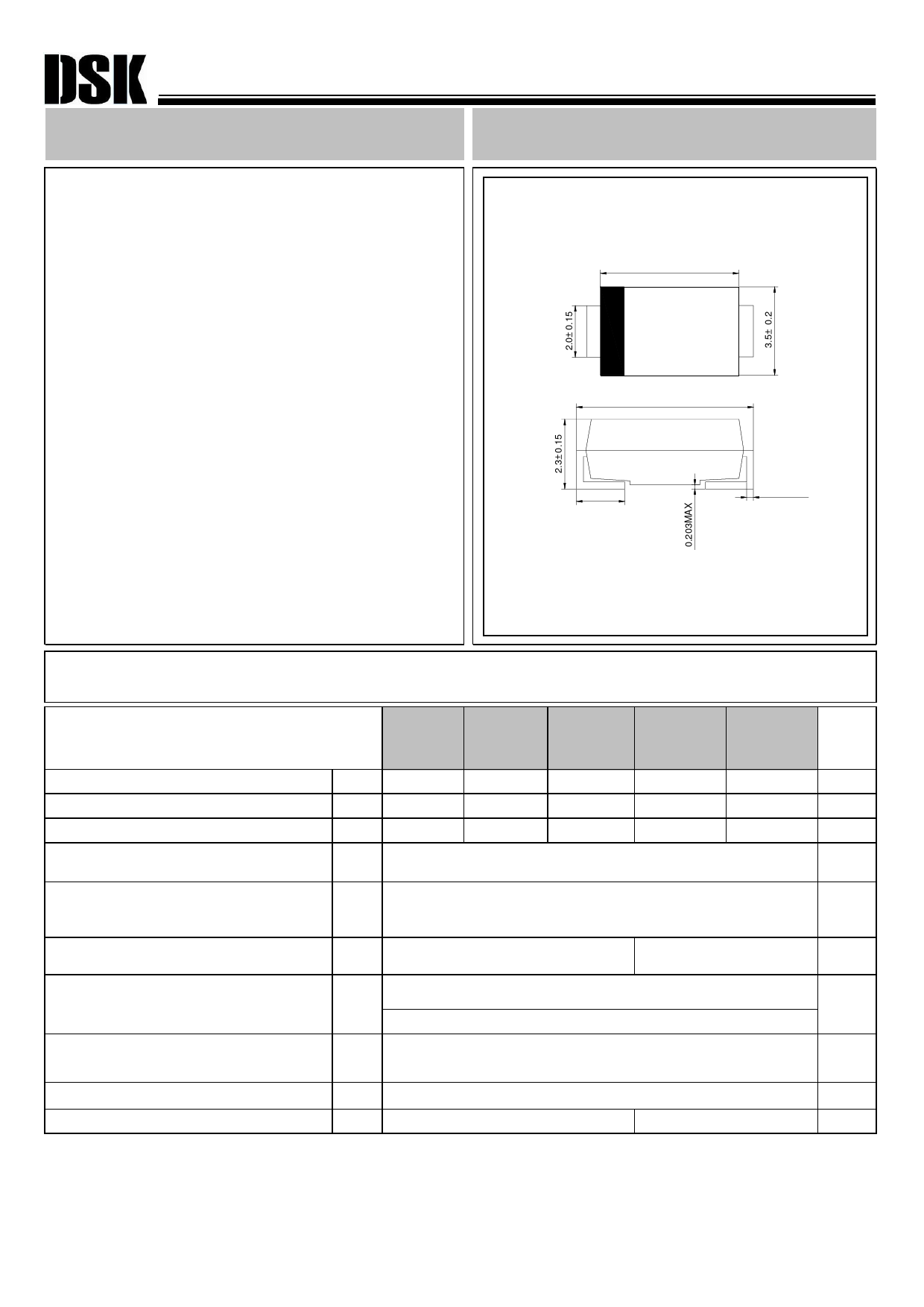
MECHANICAL DATA
◇ Case:JEDEC DO-214AA,molded plastic over
1111passivated chip
◇ Terminals:Solder Plated, solderable per MIL-STD-750,
1111Method 2026
◇ Polarity: Color band denotes cathode end
◇ Weight: 0.003 ounces, 0.093 gram
DO - 214AA(SMB)
4 . 5± 0.1 5
5 . 3± 0.2
1.25± 0.2
0.2± 0.05
Dimensions in millimeters
MAXIMUM RATINGS AND ELECTRICAL CHARACTERISTICS
Ratings at 25oC ambient temperature unless otherwise specified
B320B B330B
B340B
B350B
B360B UNITS
Maximum recurrent peak reverse voltage
VRRM
20
Maximum RMS voltage
VRWS
14
Maximum DC blocking voltage
VDC
20
Maximum average forw ord rectified current at
c TL(SEE FIG.1) (NOTE 2)
I(AV)
Peak forw ard surge current 8.3ms single half-
c sine-w ave superimposed on rated load(JEDEC IFSM
c Method)
Maximum instantaneous forw ard voltage at
v 3.0A(NOTE.1)
VF
Maximum DC reverse current @TA=25oC
IR
at rated DC blockjing voltage(NOTE1) @TA=100oC
Typical thermal resitance (NOTE2)
RθJA
RθJL
Operating junction and storage temperature range TSTG
Storage temperature range
TJ
NOTE: 1.Pulse test:300μS pulse width,1%duty cy cle
2. P.C.B.mounted with 0.55"X0.55"(14.0X14.0mm2)copper pad areas
30
40
50
21
28
35
30
40
50
3.0
60
V
42
V
60
V
A
100.0
A
0.50
0.5
-65--- +150
20
50.0
10.0
-65--- +150
0.70
V
mA
oC/W
oC
-65--- +150
oC
www.diode.kr
Share Link: 