FDPF4N60NZ_13 Просмотр технического описания (PDF) - Fairchild Semiconductor
Номер в каталоге
Компоненты Описание
производитель
FDPF4N60NZ_13 Datasheet PDF : 10 Pages
| |||
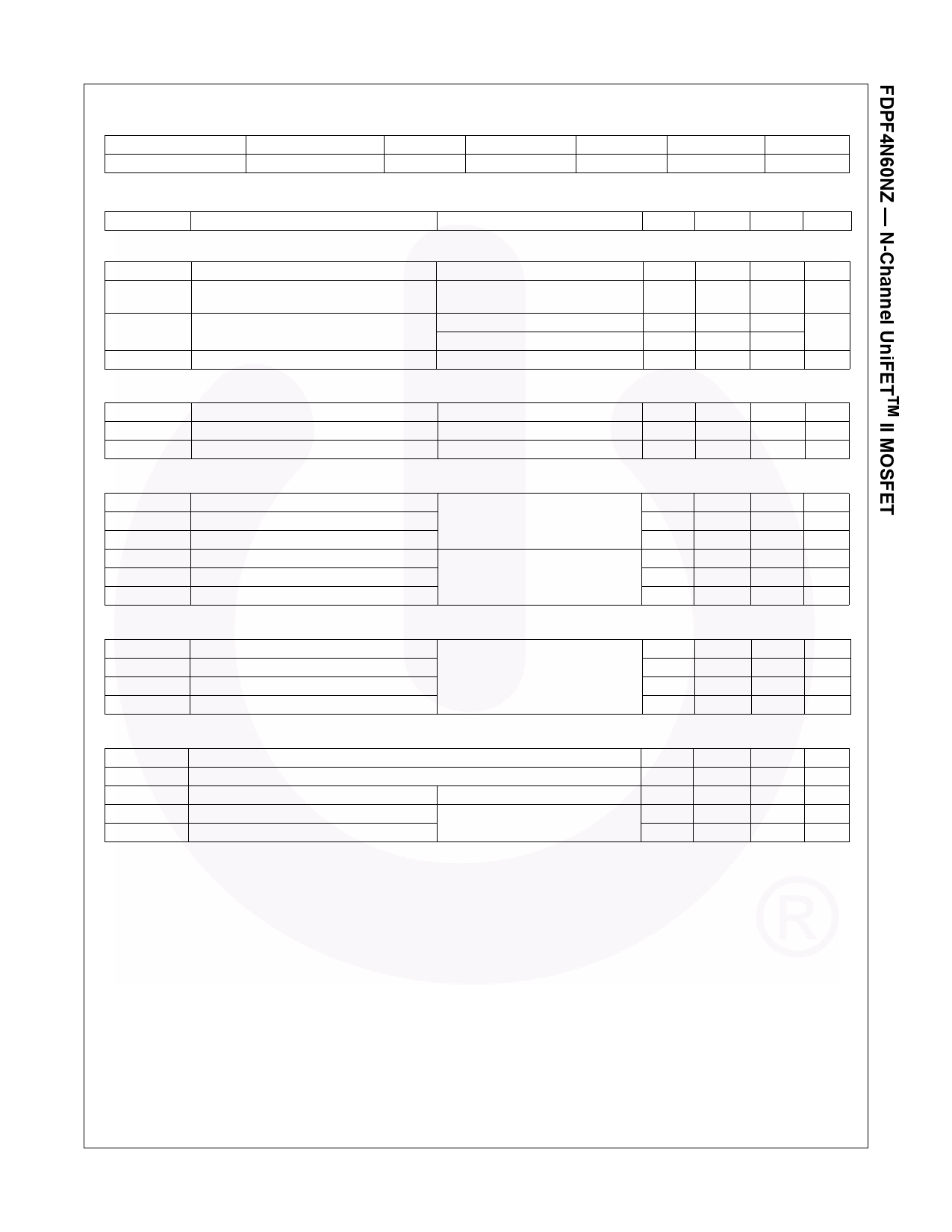
Package Marking and Ordering Information
Part Number
FDPF4N60NZ
Top Mark
FDPF4N60NZ
Package
TO-220F
Packing Method
Tube
Reel Size
N/A
Tape Width
N/A
Quantity
50 units
Electrical Characteristics TC = 25oC unless otherwise noted.
Symbol
Parameter
Test Conditions
Min.
Off Characteristics
BVDSS
ΔBVDSS
/ ΔTJ
Drain to Source Breakdown Voltage
Breakdown Voltage Temperature
Coefficient
IDSS
Zero Gate Voltage Drain Current
IGSS
Gate to Body Leakage Current
ID = 250 μA, VGS = 0 V, TC = 25oC
600
ID = 250 μA, Referenced to 25oC
-
VDS = 600 V, VGS = 0 V
-
VDS = 480 V, VGS = 0 V, TC = 125oC
-
VGS = ±25 V, VDS = 0 V
-
On Characteristics
VGS(th)
Gate Threshold Voltage
VGS = VDS, ID = 250 μA
3.0
RDS(on)
Static Drain to Source On Resistance
VGS = 10 V, ID = 1.9 A
-
gFS
Forward Transconductance
VDS = 20 V, ID = 1.9 A
-
Dynamic Characteristics
Ciss
Coss
Crss
Qg(tot)
Qgs
Qgd
Input Capacitance
Output Capacitance
Reverse Transfer Capacitance
Total Gate Charge at 10V
Gate to Source Gate Charge
Gate to Drain “Miller” Charge
VDS = 25 V, VGS = 0 V,
f = 1 MHz
VDS = 480 V ID = 3.8 A,
VGS = 10 V
-
-
-
-
-
(Note 4)
-
Switching Characteristics
td(on)
tr
td(off)
tf
Turn-On Delay Time
Turn-On Rise Time
Turn-Off Delay Time
Turn-Off Fall Time
VDD = 300 V, ID = 3.8 A,
VGS = 10 V, RG = 25 Ω
-
-
-
(Note 4)
-
Drain-Source Diode Characteristics
IS
Maximum Continuous Drain to Source Diode Forward Current
-
ISM
Maximum Pulsed Drain to Source Diode Forward Current
-
VSD
Drain to Source Diode Forward Voltage
VGS = 0 V, ISD = 3.8 A
-
trr
Reverse Recovery Time
Qrr
Reverse Recovery Charge
VGS = 0 V, ISD = 3.8 A,
-
dIF/dt = 100 A/μs
-
Typ.
-
0.6
-
-
-
-
1.9
3.3
385
40
3.7
8.3
2.1
3.3
12.7
15.1
30.2
12.8
-
-
-
168
0.7
Max. Unit
-
V
-
V/oC
1
10
μA
±10
μA
5.0
V
2.5
Ω
-
S
510
pF
60
pF
5
pF
10.8 nC
-
nC
-
nC
35.4
ns
40.2
ns
70.4
ns
35.6
ns
3.8*
A
15
A
1.4
V
-
ns
-
μC
Notes:
1. Repetitive rating: pulse-width limited by maximum junction temperature.
2. L = 31 mH, IAS = 3.8 A, VDD = 50 V, RG = 25 Ω, starting TJ = 25°C.
3. ISD ≤ 3.8 A, di/dt ≤ 200 A/μs, VDD ≤ BVDSS, starting TJ = 25°C.
4. Essentially independent of operating temperature typical characteristics.
©2011 Fairchild Semiconductor Corporation
2
FDPF4N60NZ Rev. C1
www.fairchildsemi.com
Share Link: 