NC7SZ08M5X_NL Просмотр технического описания (PDF) - Fairchild Semiconductor
Номер в каталоге
Компоненты Описание
производитель
NC7SZ08M5X_NL Datasheet PDF : 12 Pages
| |||
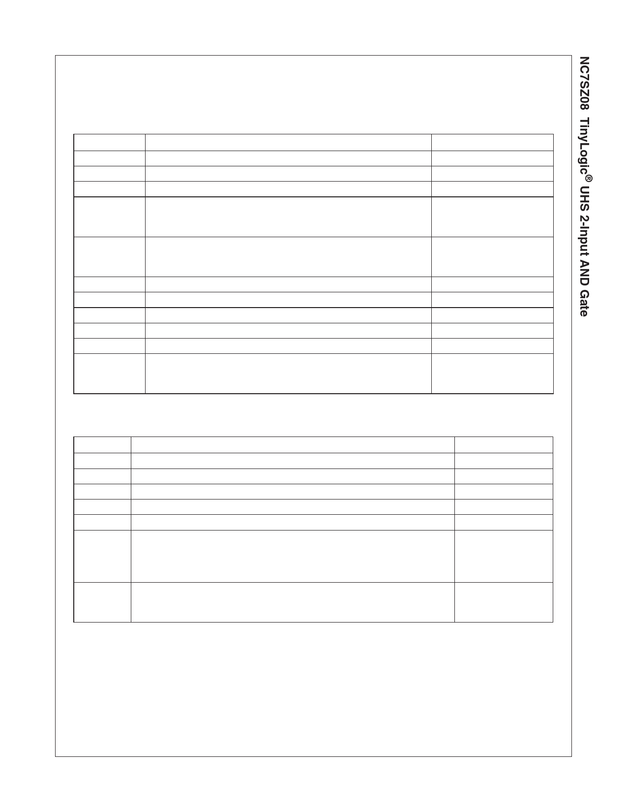
Absolute Maximum Ratings
The “Absolute Maximum Ratings” are those values beyond which the safety of the device cannot be guaranteed.
The device should not be operated at these limits. The parametric values defined in the Electrical Characteristics tables
are not guaranteed at the absolute maximum ratings. The “Recommended Operating Conditions” table will define the
conditions for actual device operation.
Symbol
Parameter
Rating
VCC
VIN
VOUT
IIK
IOK
IOUT
ICC/ IGND
TSTG
TJ
TL
PD
Supply Voltage
DC Input Voltage
DC Output Voltage
DC Input Diode Current
@ VIN < -0.5V
@ VIN > 6V
DC Output Diode Current
@ VOUT < -0.5V
@ VOUT > 6V, VCC = GND
DC Output Current
DC VCC/ GND Current
Storage Temperature
Junction Temperature under Bias
Junction Lead Temperature (Soldering, 10 seconds)
Power Dissipation @ +85°C
SOT23-5
SC70-5
-0.5V to +6V
-0.5V to +6V
-0.5V to +6V
-50mA
+20mA
-50mA
+20mA
±50mA
±50mA
-65°C to +150°C
150°C
260°C
200mW
150mW
Recommended Operating Conditions(3)
Symbol
VCC
VCC
VIN
VOUT
TA
tr, tf
θ JA
Parameter
Supply Voltage Operation
Supply Voltage Data Retention
Input Voltage
Output Voltage
Operating Temperature
Input Rise and Fall Time
VCC = 1.8V, 2.5V ±0.2V
VCC = 3.3V ±0.3V
VCC = 5.0V ±0.5V
Thermal Resistance
SOT23-5
SC70-5
Notes:
3. Unused inputs must be held HIGH or LOW. They may not float.
Rating
1.65V to 5.5V
1.5V to 5.5V
0V to 5.5V
0V to VCC
-40°C to +85°C
0ns/V to 20ns/V
0ns/V to 10ns/V
0ns/V to 5ns/V
300°C/W
425°C/W
3
NC7SZ08 Rev. 1.0.0
www.fairchildsemi.com
Share Link: 