QL7100-6PB516I Просмотр технического описания (PDF) - QuickLogic Corporation
Номер в каталоге
Компоненты Описание
производитель
QL7100-6PB516I Datasheet PDF : 65 Pages
| |||
EclipsePlus Family Data Sheet
• • • • • • Combining Performance, Density, and Embedded RAM
Device Highlights
Flexible Programmable Logic
• 0.25 µm five layer metal CMOS process
• 2.5 V VCC, 2.5/3.3 V drive capable I/O
• Up to 4,032 logic cells
• Up to 583,008 system gates
• Up to 347 I/O pins
Embedded Dual-Port SRAM
• Up to thirty-six 2,304-bit dual-port high
performance SRAM blocks
• Up to 82,900 RAM bits
• RAM/ROM/FIFO wizard for automatic
configuration
• Configurable and cascadable
Programmable I/O
• High performance enhanced I/O (EIO)—
less than 3 ns Tco
• Programmable slew rate control
• Programmable I/O standards:
LVTTL, LVCMOS, PCI, GTL+, SSTL2,
and SSTL3
Eight independent I/O banks
Three register configurations: input, output,
and output enable
Advanced Clock Network
• Nine global clock networks:
One dedicated
Eight programmable
• 20 quad-net networks—five per quadrant
• 16 I/O controls—two per I/O bank
• Four phase locked loops
Embedded Computational Units
ECUs provide integrated multiply, add, and
accumulate functions.
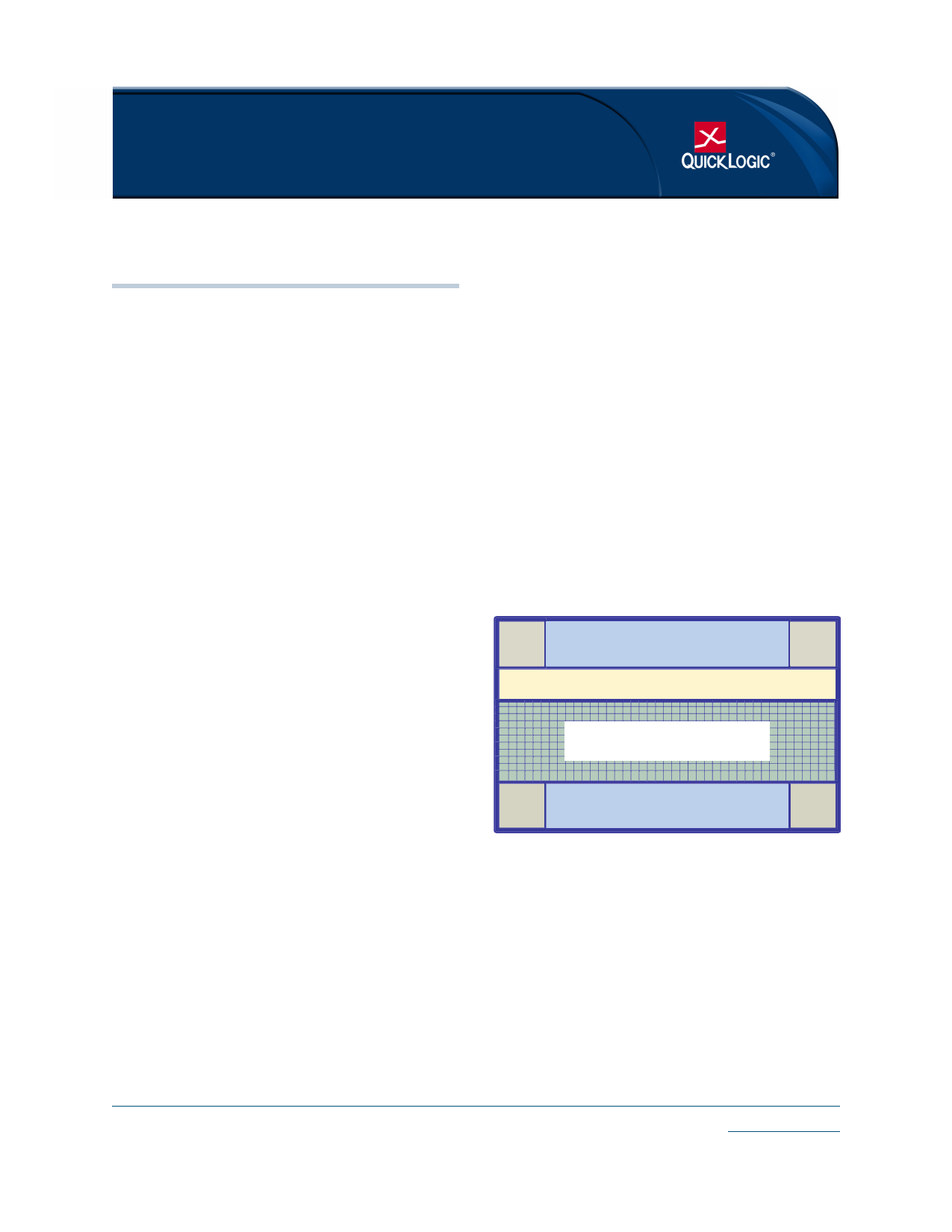
Figure 1: EclipsePlus Block Diagram
PLL
Memory - Dual Port RAM
PLL
Embedded Computational Units
High Speed Logic Cells
583K Gates
PLL
Memory - Dual Port RAM
PLL
© 2006 QuickLogic Corporation
www.quicklogic.com
•
•••
••
1
Share Link: 