MAX77179 Просмотр технического описания (PDF) - Maxim Integrated
Номер в каталоге
Компоненты Описание
производитель
MAX77179
Maxim Integrated
MAX77179 Datasheet PDF : 17 Pages
| |||
MAX77178 / MAX77179
High-Bandwidth LTE/WCDMA PA Power Management ICs
in a 1.75mm x 1.4mm, 0.4mm Pitch WLP
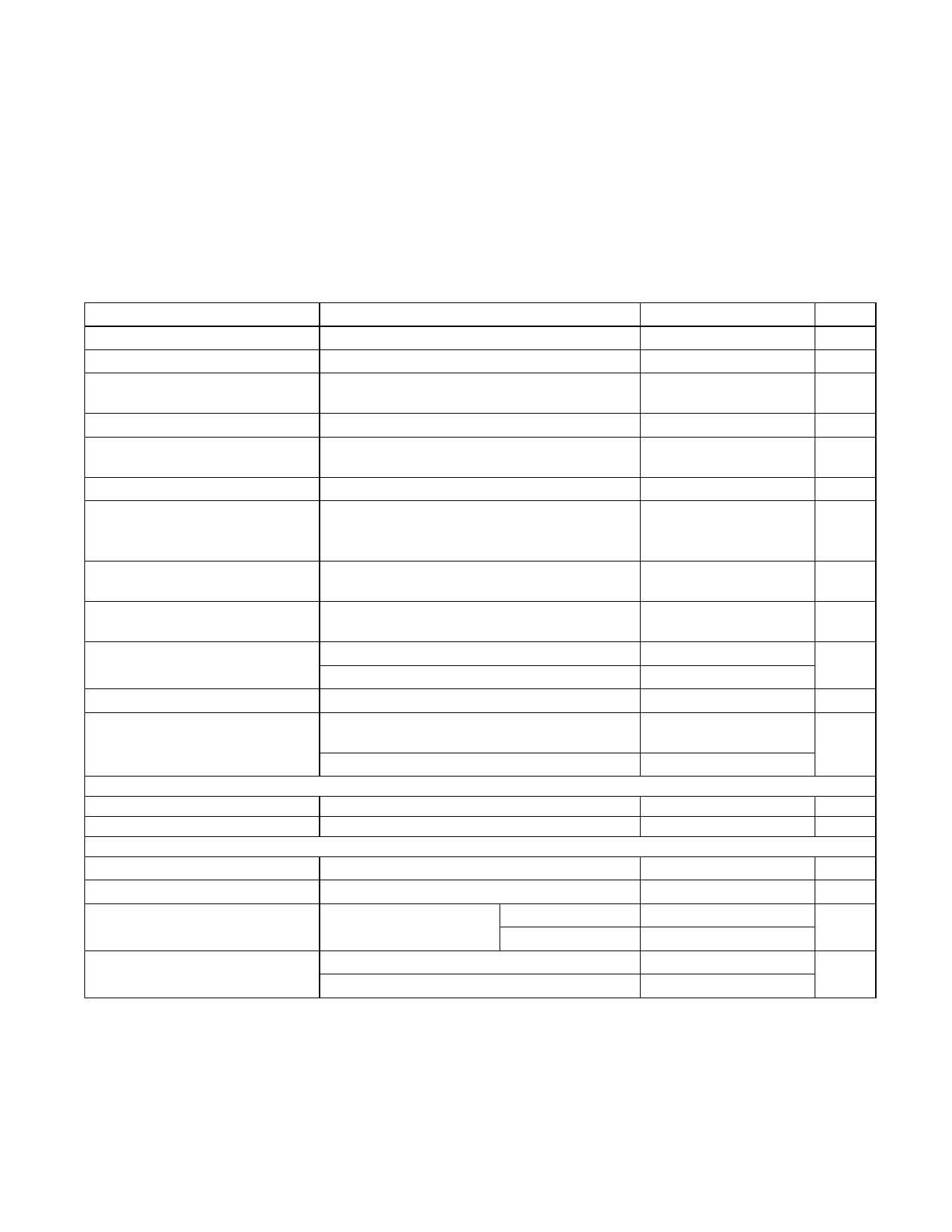
ELECTRICAL CHARACTERISTICS (continued)
(VIN1 = VIN2 = VIN3 = 3.7V, VPGND = VAGND = 0V, L = 0.47µH, COUT = 4.7µF, TA = -40°C to +85°C. Typical values are at
TA = +25°C, unless otherwise noted.) (Note 3)
PARAMETER
LX Rise Time
Output-Voltage Line Regulation
Line Regulation Transient Response
Output-Voltage Load Regulation
Load Regulation Transient Response
Operating Frequency
Automatic Bypass Mode Entry
Threshold
Automatic Bypass Mode Entry
Hysteresis
Automatic Bypass Mode Exit
Debounce Time
Minimum Duty Cycle
Maximum Duty Cycle
Output-Voltage Ripple
PROTECTION CIRCUITS
Thermal Shutdown
Thermal Shutdown Hysteresis
CONTROL
REF Input Voltage Range
REF to OUT Gain Accuracy
REF to OUT Absolute Accuracy
(MAX77179)
Output Voltage Range (MAX77179)
CONDITIONS
VIN = 2.5V to 5.5V, IOUT = 100mA, VOUT = 1.8V
VIN1(DC) = 3.6VRMS, VIN1(AC) = 300mVP-P ripple
at 10Hz to 270kHz, IOUT = 500mA, VOUT = 3.0V
IOUT = 0 to 1A
tRISE = tFALL = 1.5Fs, IOUT = 0.2A to 1A,
VOUT = 3.0V
VOUT = 1.8V, IOUT = 0A, PWM
VIN - VOUT, when the drop between VIN and VOUT
becomes less than this threshold, high-side FET is
turned on continuously
Skip mode
PWM mode
COUT = 4.7FF, ESR of COUT < 20mI, fSW = 8MHz,
IOUT = 10mA to 1A, VOUT = 1.8V, PWM mode
Skip mode, IOUT = 0mA
MAX77179, analog control voltage
MAX77179, VREF = 1V, gain = VOUT/VREF
VREF = 1V, IOUT = 0
TA = +25NC
TA = -40NC to +85NC
Controlled by the REF input
VREF = 0V, skip mode operation
MIN
6
0
-2.5
-3
-3.5
0.5
TYP MAX UNITS
1
ns
1.3
%/V
25
mVP-P
-1.5
%/A
25
mVP-P
8
10
MHz
0.125
V
40
mV
5
Fs
0
%
10
100
%
5
mVP-P
45
160
NC
20
NC
VIN3 - 0.3
V
+2.5
%
+3
%
+3.5
VIN
V
0.1
Maxim Integrated
4
Share Link: 