TLE4307DV33 Просмотр технического описания (PDF) - Infineon Technologies
Номер в каталоге
Компоненты Описание
производитель
TLE4307DV33 Datasheet PDF : 10 Pages
| |||
TLE 4307
I1
SL 4
TLE 4307
Power
Charge
Pump
Very
Low-Drop
5Q
Regulator
2
3
C
GND
AES02793
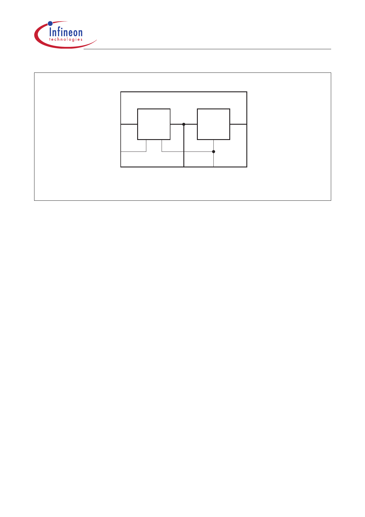
Figure 2 Block Diagram
Circuit Description
The TLE 4307 consists of 2 stages, the charge pump and the very low drop voltage
regulator.
Charge Pump
The power stage is used as a switching element, that is driven by a buffer. A current
source keeps the power stage on. When the output C of the charge pump reaches VC,off,
the power stage is switched off. It is active clamped, when the input I reaches VI,cl.
Optional, an external capacity can be connected between pin SL and I to limit the slew
rate at the input, when an inductive load drives the IC. Saturation control as a function of
the load current prevents any over-saturation of the power element. The regulator is
additionally protected against overload and overtemperature.
Very Low Drop Regulator
The control amplifier compares a reference voltage, made highly accurate by resistance
balancing, with a voltage proportional to the output voltage and drives the base of the
series PNP transistor via a buffer. Saturation control as a function of the load current
prevents any over-saturation of the power element. The regulator is additionally
protected against overload and overtemperature.
Data Sheet Rev. 1.1
3
2000-10-11
Share Link: 