NCV7518MWTXG Просмотр технического описания (PDF) - ON Semiconductor
Номер в каталоге
Компоненты Описание
производитель
NCV7518MWTXG Datasheet PDF : 37 Pages
| |||
NCV7518, NCV7518A
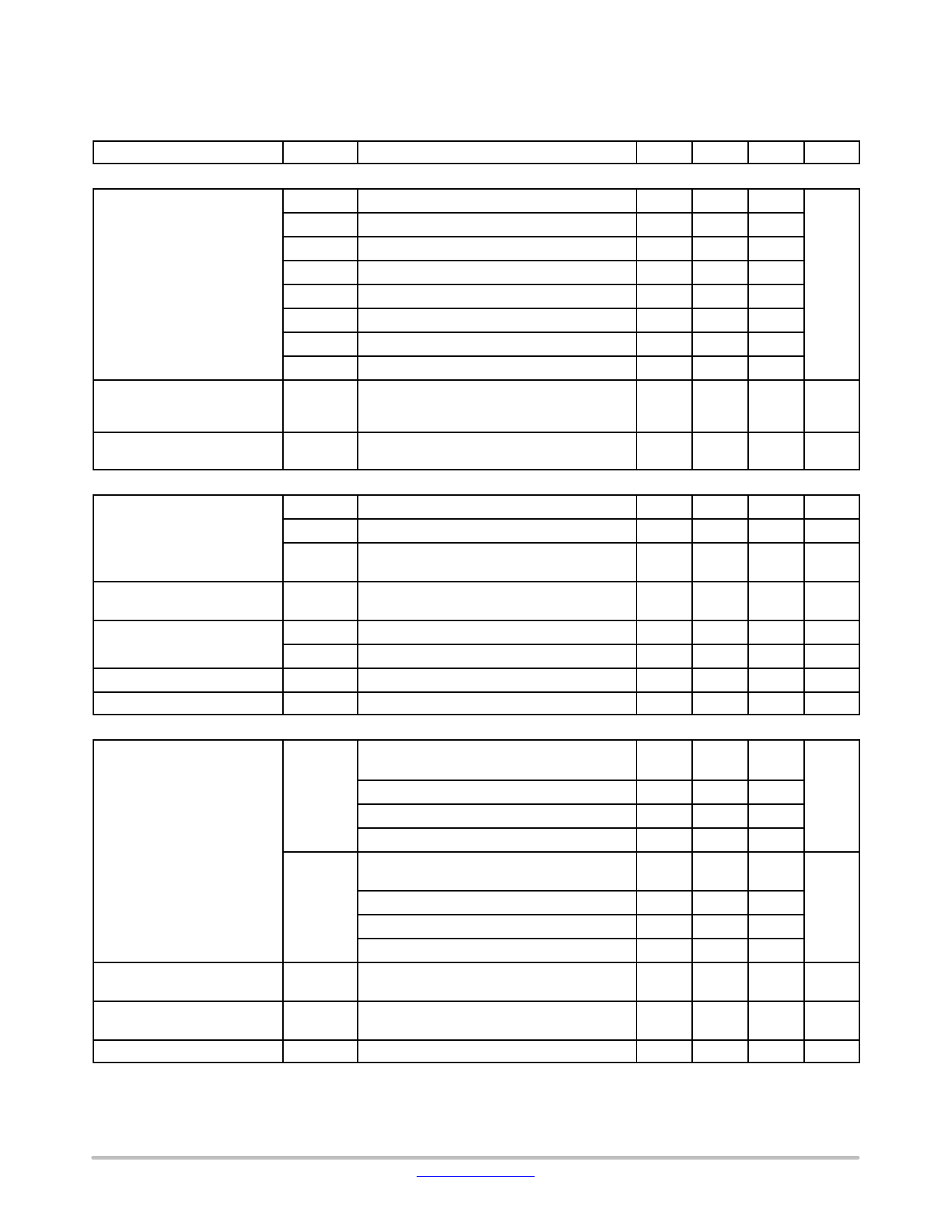
ELECTRICAL CHARACTERISTICS (continued)
(4.75 V ≤ VCCX ≤ 5.25 V, VDD = VCCX, 4.5 V ≤ VLOAD ≤ 18 V, RSTB = VCCX, ENB = 0, −40°C ≤ TJ ≤ 150°C, unless otherwise specified.)
(Note 7)
Characteristic
Symbol
Conditions
Min
Typ
Max
Unit
FAULT DETECTION − GATX ON
DRNX Shorted Load Threshold
VFLTREF = 0.35V
DRNX Input Leakage Current
V25
V40
V50
V60
V70
V80
V90
V100
IDLKG
DRNX Clamp Voltage
VCL
Register R2.C[11:9] = 000 (DEFAULT)
Register R2.C[11:9] = 001
Register R2.C[11:9] = 010
Register R2.C[11:9] = 011
Register R2.C[11:9] = 100
Register R2.C[11:9] = 101
Register R2.C[11:9] = 110
Register R2.C[11:9] = 111
0 V ≤ VCC1 = VCC2 = VDD ≤ 5.25 V,
RSTB = 0 V, VDRNX = 32 V
TA ≤ 25°C
IDRNX= ICL(MAX) =10 mA; Transient
(≤2 ms, ≤1% Duty)
20
25
30
%
35
40
45
VFLTREF
45
50
55
55
60
65
65
70
75
75
80
85
85
90
95
95
100
105
−5.0
−
−1.0
−
mA
5.0
1.0
60
−
78
V
Fault Detection − GATX OFF (7.5 V ≤ VLOAD ≤ 18 V, Register R3.D[11:0] = 1)
DRNX Diagnostic Current
− Proportional to VLOAD
ISG
Short to GND Detection, VDRNX = 43%VLOAD
IOL
Open Load Detection, VDRNX = 61%VLOAD
ICHG
Transient Fast Charge Current,
0 < VDRNX < VCTR, t < tBL(OFF)
Diagnostic Current Limit Point
VLIM
Current Clamped and No Longer Proportional to
VLOAD
DRNX Fault Threshold Voltage
VSG
Short to GND Detection
VOL
Open Load Detection
DRNX Off State Bias Voltage
VCTR
VLOAD Undervoltage Threshold VLDUV
VLOAD Decreasing
FAULT TIMERS
− 81
2.73
−270
20
39.56
56.12
46.92
4.1
−60
4.20
−200
−
43
61
51
6.3
− 39
5.67
−130
mA / V
mA / V
mA / V
−
V
46.44
65.88
55.08
7.5
%VLOAD
%VLOAD
%VLOAD
V
Channel Fault Blanking Timers
tBL(ON)
VDRNX = VLOAD; INX rising to FLTB Falling
4.8
6
7.2
ms
(Figure 6)
Register R2.C[6:5] = 00
Register R2.C[6:5] = 01
9.6
12
14.4
Register R2.C[6:5] = 10 (DEFAULT)
19.2
24
28.8
Register R2.C[6:5] = 11
28.8
48
57.6
tBL(OFF)
VDRNX = 0V; INX falling to FLTB Falling
Register R2.C[8:7] = 00
44
55
66
ms
Register R2.C[8:7] = 01
65
81
97
Register R2.C[8:7] = 10 (DEFAULT)
130
162
195
Register R2.C[8:7] = 11
260
325
390
Channel Fault Filter Timer
(Figure 7)
Global Fault Retry Timer
(Figure 8)
tFF(ON)
tFF(OFF)
tFR
Register R0.M[5:0] = 1
2.0
3.0
4.0
ms
44
55
66
6
8
10
ms
Timer Clock
fCLK
RSTB = VCC1
−
4.0
−
MHz
7. Min/Max values are valid for the temperature range −40°C ≤ TJ ≤ 150°C unless noted otherwise. Min/Max values are guaranteed by test,
design or statistical correlation.
8. Guaranteed by design.
www.onsemi.com
7
Share Link: 