SI7013-A10 Просмотр технического описания (PDF) - Silicon Laboratories
Номер в каталоге
Компоненты Описание
производитель
SI7013-A10 Datasheet PDF : 46 Pages
| |||
Si7013-A10
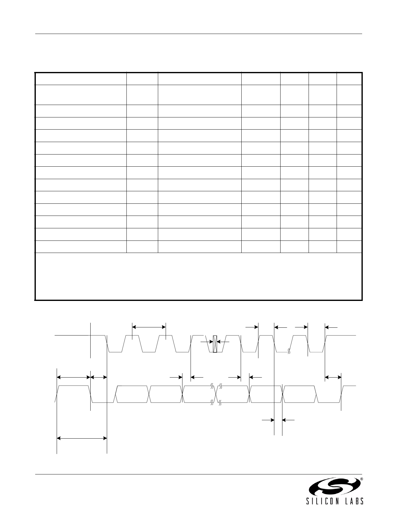
Table 3. I2C Interface Specifications1
1.9 VDD 3.6 V; TA = –40 to +85 °C (G grade) or –40 to +125 °C (I/Y grade) unless otherwise noted.
Parameter
Symbol
Test Condition
Min
Typ Max Unit
Hysteresis
VHYS High-to-low versus low-to- 0.05 x VDD —
—
V
high transition
SCLK Frequency2
fSCL
—
SCL High Time
tSKH
0.6
SCL Low Time
tSKL
1.3
Start Hold Time
tSTH
0.6
Start Setup Time
tSTS
0.6
Stop Setup Time
tSPS
0.6
Bus Free Time
tBUF
Between Stop and Start
1.3
SDA Setup Time
tDS
100
SDA Hold Time
tDH
100
SDA Valid Time
tVD;DAT From SCL low to data valid
—
SDA Acknowledge Valid Time tVD;ACK From SCL low to data valid
—
Suppressed Pulse Width3
tSP
50
—
400 kHz
—
—
µs
—
—
µs
—
—
µs
—
—
µs
—
—
µs
—
—
µs
—
—
ns
—
—
ns
—
0.9
µs
—
0.9
µs
—
—
ns
Notes:
1. All values are referenced to VIL and/or VIH.
2. Depending on the conversion command, the Si7013 may hold the master during the conversion (clock stretch). At
above 300 kHz SCL, the Si7013 may hold the master briefly for user register and device ID transactions. At the highest
I2C speed of 400 kHz the stretching will be <10 µs.
3. Pulses up to and including 50ns will be suppressed.
SCL
tBUF
tSTH
1/fSCL
tSKH
tSP
tDS
tDH
tSKL
tSPS
SDA
Start Bit
D7
D6
D5
D0
R/W
ACK
Stop Bit
tSTS
tVD : ACK
Figure 1. I2C Interface Timing Diagram
6
Rev. 1.0
Share Link: 