SST25VF032B Просмотр технического описания (PDF) - Microchip Technology
Номер в каталоге
Компоненты Описание
производитель
SST25VF032B Datasheet PDF : 33 Pages
| |||
A Microchip Technology Company
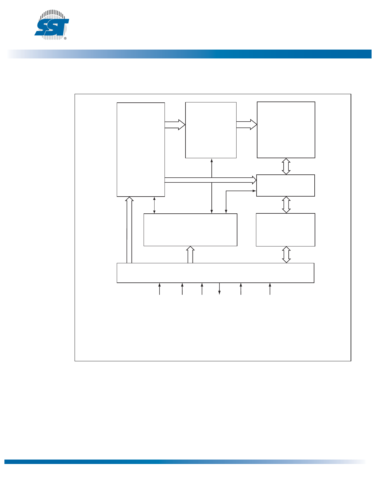
Block Diagram
32 Mbit SPI Serial Flash
SST25VF032B
Data Sheet
Address
Buffers
and
Latches
X - Decoder
SuperFlash
Memory
Y - Decoder
Control Logic
I/O Buffers
and
Data Latches
Serial Interface
CE# SCK SI SO WP# HOLD#
1327 B1.0
Note: In AAI mode, the SO pin can act as a RY/BY# pin when configured as a ready/busy status pin. See “End-of-
Write Detection” on page 12. for details
Figure 1: Functional Block Diagram
©2011 Silicon Storage Technology, Inc.
3
DS25071A
12/11
Share Link: 