CY7C1648KV18(2018) Просмотр технического описания (PDF) - Cypress Semiconductor
Номер в каталоге
Компоненты Описание
производитель
CY7C1648KV18
(Rev.:2018)
(Rev.:2018)
Cypress Semiconductor
CY7C1648KV18 Datasheet PDF : 29 Pages
| |||
CY7C1648KV18
CY7C1650KV18
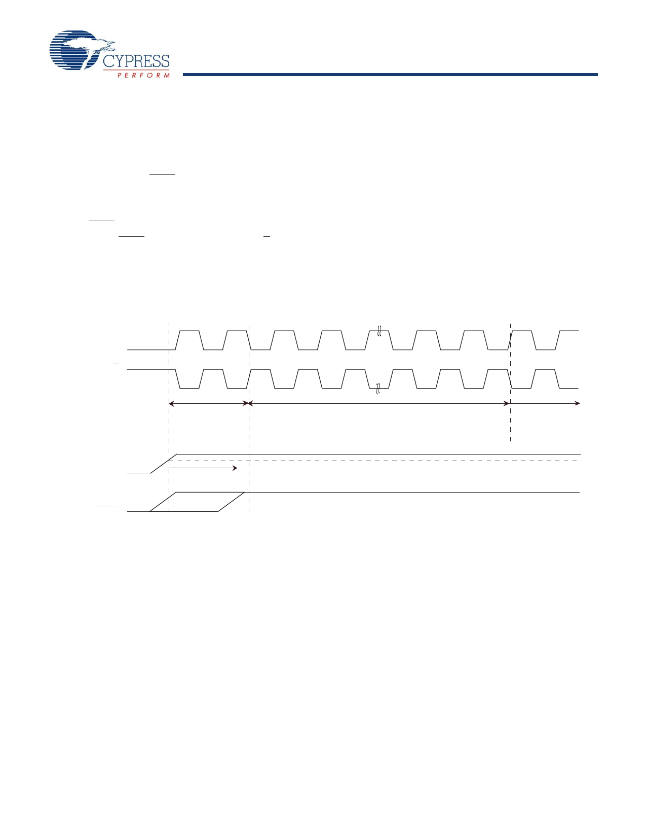
Power Up Sequence in DDR II+ SRAM
DDR II+ SRAMs must be powered up and initialized in a
predefined manner to prevent undefined operations.
Power Up Sequence
■ Apply power and drive DOFF either high or low (all other inputs
can be high or low).
❐ Apply VDD before VDDQ.
❐ Apply VDDQ before VREF or at the same time as VREF.
❐ Drive DOFF high.
■ Provide stable DOFF (high), power and clock (K, K) for 20 s
to lock the PLL
PLL Constraints
■ PLL uses K clock as its synchronizing input. The input must
have low phase jitter, which is specified as tKC Var.
■ The PLL functions at frequencies down to 120 MHz.
■ If the input clock is unstable and the PLL is enabled, then the
PLL may lock onto an incorrect frequency, causing unstable
SRAM behavior. To avoid this, provide 20 s of stable clock to
relock to the desired clock frequency.
Figure 4. Power Up Waveforms
K
K
VDD/ VDDQ
DOFF
Unstable Clock
> 20μs Stable clock
Clock Start (Clock Starts after VDD / VDDQ Stable)
VDD / VDDQ Stable (< +/- 0.1V DC per 50ns )
Fix HIGH (or tie to VDDQ)
Start Normal
Operation
Document Number: 001-44061 Rev. *L
Page 18 of 29
Share Link: 