AD7091R-2BCPZ-RL7 Просмотр технического описания (PDF) - Analog Devices
Номер в каталоге
Компоненты Описание
производитель
AD7091R-2BCPZ-RL7 Datasheet PDF : 42 Pages
| |||
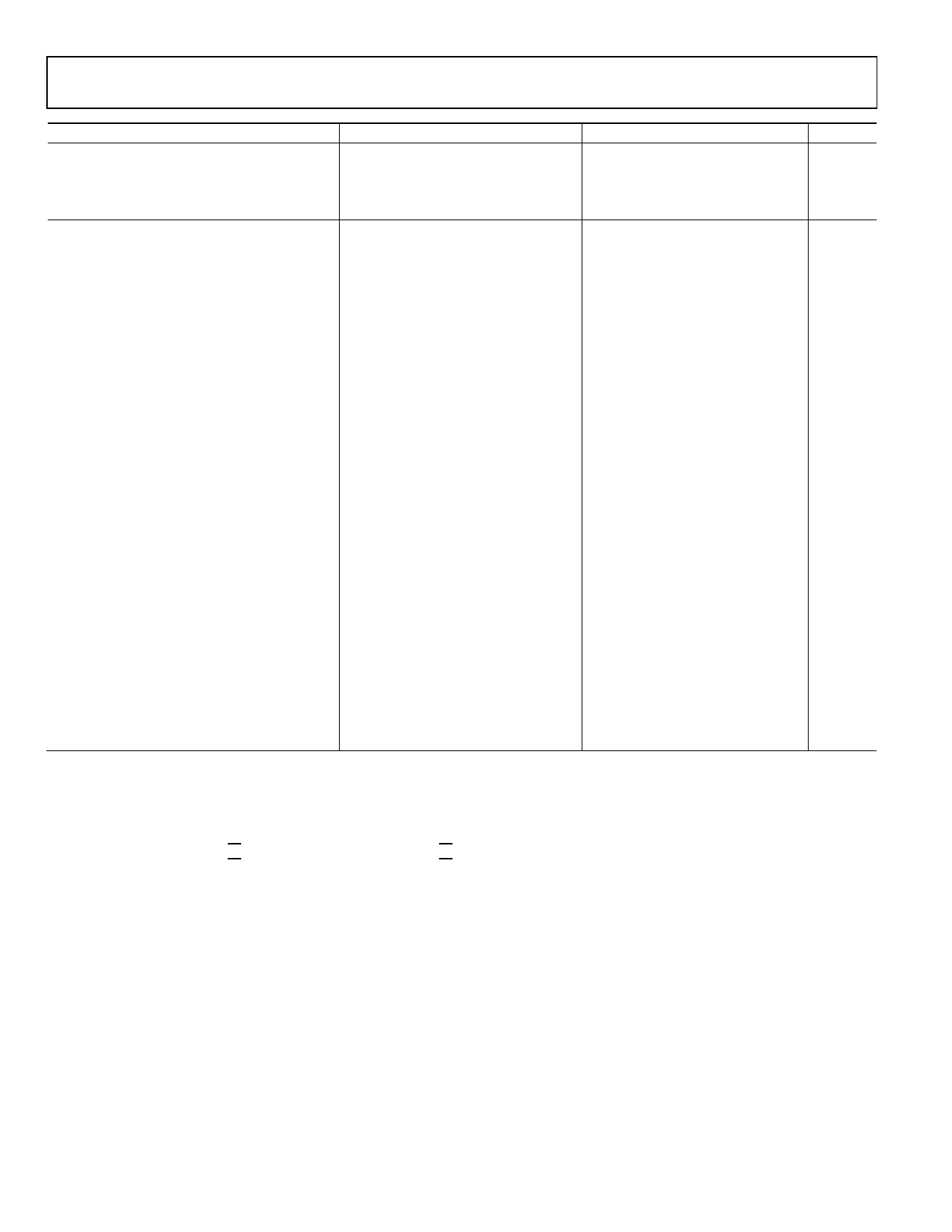
AD7091R-2/AD7091R-4/AD7091R-8
Data Sheet
Parameter
CONVERSION RATE
Conversion Time
Transient Response
Throughput Rate
POWER REQUIREMENTS
VDD
VDRIVE
VDRIVE Range4
IDD
Normal Mode—Static5
Normal Mode—Operational
Power-Down Mode
IDRIVE
Normal Mode—Static6
Normal Mode—Operational
Power-Down Mode
Total Power Dissipation7
Normal Mode—Static
Normal Mode—Operational
Power-Down Mode
Test Conditions/Comments
Min
Full-scale step input
2.7
Specified performance
2.7
Functional
1.8
VIN = 0 V
VDD = 5.25 V
VDD = 3 V
VDD = 5.25 V, fSAMPLE = 1 MSPS
VDD = 3 V, fSAMPLE = 1 MSPS
VDD = 5.25 V
VDD = 5.25 V, TA = −40°C to +85°C
VDD = 3 V
VIN = 0 V
VDRIVE = 5.25 V
VDRIVE = 3 V
VDRIVE = 5.25 V, fSAMPLE = 1 MSPS
VDRIVE = 3 V, fSAMPLE = 1 MSPS
VDRIVE = 5.25 V
VDRIVE = 3 V
VIN = 0 V
VDD = VDRIVE = 5.25 V
VDD = VDRIVE = 3 V
VDD = VDRIVE = 5.25 V, fSAMPLE = 1 MSPS
VDD = VDRIVE = 3 V, fSAMPLE = 1 MSPS
VDD = VDRIVE = 3 V, fSAMPLE = 100 SPS
VDD = 5.25 V
VDD = 5.25 V, TA = −40°C to +85°C
VDD = VDRIVE = 3 V
Typ Max
600
400
1
5.25
5.25
5.25
22
50
21.6 46
500 570
450 530
0.550 17
0.550 6
0.435 15
2
4
1
3.5
30
70
10
15
1
1
0.130
0.070
2.8
1.4
0.080
3
3
1.4
0.290
0.149
3.4
1.7
95
33
50
Unit
ns
ns
MSPS
V
V
V
µA
µA
µA
µA
µA
µA
µA
µA
µA
µA
µA
µA
µA
mW
mW
mW
mW
mW
µW
µW
µW
1 Multiplexer input voltage should not exceed VDD.
2 Sample tested during initial release to ensure compliance.
3 When referring to a single function of a multifunction pin in the parameters, only the portion of the pin name that is relevant to the specification is listed. For full pin
names of multifunction pins, refer to the Pin Configurations and Function Descriptions section.
4 Device is functional and meets dynamic performance/dc accuracy specifications with VDRIVE down to 1.8 V, but the device is not capable of achieving a throughput of
1 MSPS.
5 SCLK operates in burst mode, and CS idles high. With a free running SCLK and CS pulled low, the IDD static current is increased by 30 µA typical at VDD = 5.25 V.
6 SCLK operates in burst mode, and CS idles high. With a free running SCLK and CS pulled low, the IDRIVE static current is increased by 32 µA typical at VDRIVE = 5.25 V.
7 Total power dissipation includes contributions from VDD, VDRIVE, and REFIN (see Note 2).
Rev. C | Page 4 of 42
Share Link: 