ISPLSI3256E-100LB320 Просмотр технического описания (PDF) - Lattice Semiconductor
Номер в каталоге
Компоненты Описание
производитель
ISPLSI3256E-100LB320 Datasheet PDF : 15 Pages
| |||
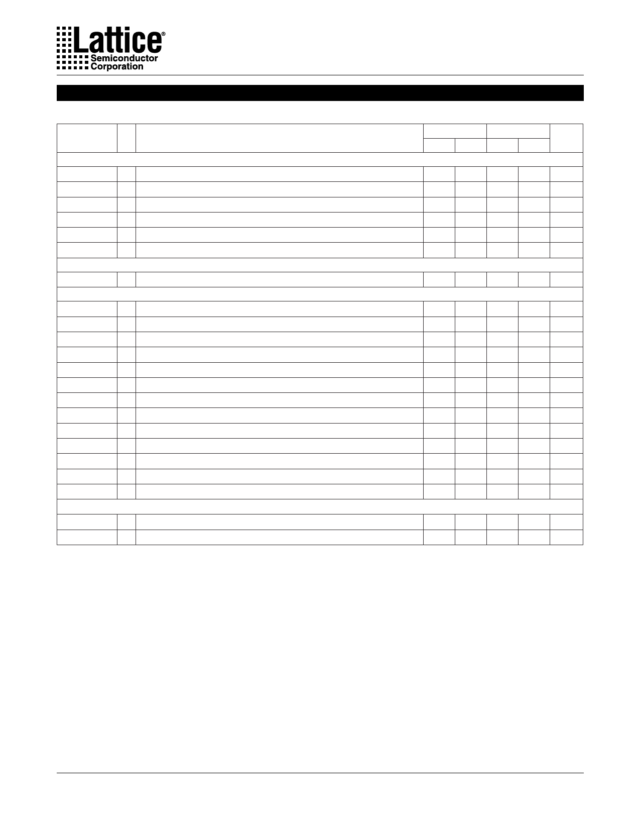
Specifications ispLSI 3256E
Internal Timing Parameters1
Over Recommended Operating Conditions
PARAMETER #2
DESCRIPTION
Inputs
tiobp
24 I/O Register Bypass
tiolat
25 I/O Latch Delay
tiosu
26 I/O Register Setup Time before Clock
tioh
27 I/O Register Hold Time after Clock
tioco
28 I/O Register Clock to Out Delay
tior
29 I/O Register Reset to Out Delay
GRP
tgrp
30 GRP Delay
GLB
t4ptbp
31 4 Product Term Bypass Path Delay (Comb.)
t4ptbr
32 4 Product Term Bypass Path Delay (Reg.)
t1ptxor
33 1 Product Term/XOR Path Delay
t20ptxor
34 20 Product Term/XOR Path Delay
txoradj
35 XOR Adjacent Path Delay3
tgbp
36 GLB Register Bypass Delay
tgsu
37 GLB Register Setup Time before Clock
tgh
38 GLB Register Hold Time after Clock
tgco
39 GLB Register Clock to Output Delay
tgro
40 GLB Register Reset to Output Delay
tptre
41 GLB Product Term Reset to Register Delay
tptoe
42 GLB Product Term Output Enable to I/O Cell Delay
tptck
43 GLB Product Term Clock Delay
ORP
torp
44 ORP Delay
torpbp
45 ORP Bypass Delay
1. Internal Timing Parameters are not tested and are for reference only.
2. Refer to Timing Model in this data sheet for further details.
3. The XOR adjacent path can only be used by hard macros.
Timing Int.3256E.eps
-100
-70
UNITS
MIN. MAX. MIN. MAX.
— 2.4 — 4.0 ns
— 10.3 — 14.0 ns
4.8 — 5.8 — ns
-1.6 — -2.5 — ns
— 5.8 — 8.5 ns
— 5.8 — 7.5 ns
— 2.3 — 3.2 ns
— 3.2 — 3.6 ns
— 3.1 — 4.8 ns
— 4.0 — 5.1 ns
— 4.1 — 5.2 ns
— 4.3 — 5.7 ns
— 1.5 — 1.6 ns
0.3 — 1.2 — ns
5.0 — 7.6 — ns
— 1.6 — 3.0 ns
— 5.2 — 5.2 ns
— 4.0 — 4.4 ns
— 6.5 — 6.9 ns
3.0 3.6 3.4 4.2 ns
— 1.2 — 1.9 ns
— 0.7 — 0.9 ns
7
Share Link: 