ADT7310TRZ-REEL7(2009) Просмотр технического описания (PDF) - Analog Devices
Номер в каталоге
Компоненты Описание
производитель
ADT7310TRZ-REEL7 Datasheet PDF : 24 Pages
| |||
ADT7310
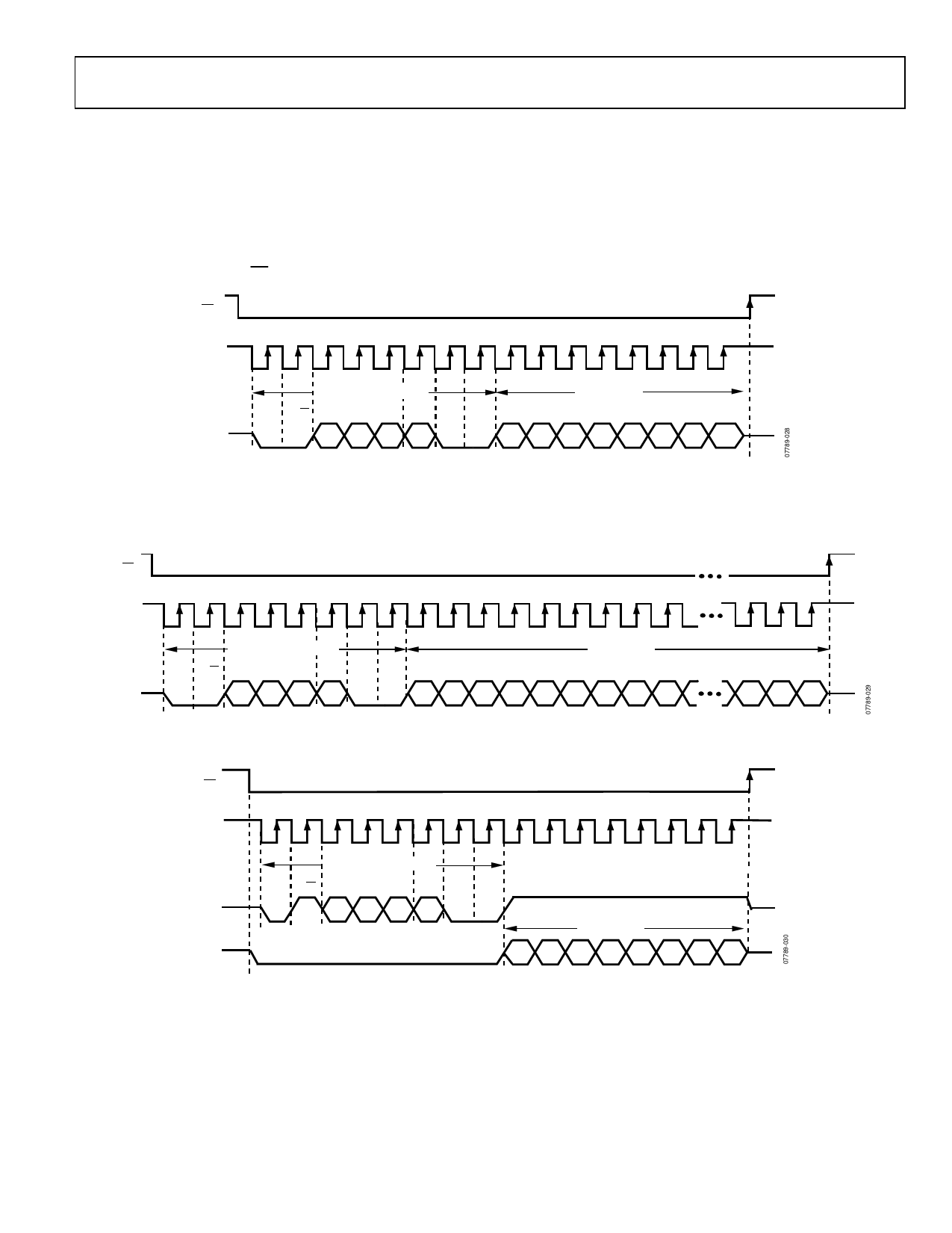
CS
SCLK
DIN
DOUT
1
2
3
4
5
6
7
8
9 10 11 12 13 14 15 16 17
8-BIT COMMAND BYTE
0
R/W
CONT
REGISTER ADDR READ
0
0
C7 C6 C5 C4 C3 C2 C1 C0
16-BIT DATA
D15 D14 D13 D12 D11 D10 D9 D8 D7
Figure 21. Read from a 16-Bit Register
22 23 24
D2 D1 D0
READING DATA
A read transaction begins when the master writes the command
byte to the ADT7310 with the read/write bit set to 1. The master
then supplies 8 or 16 clock pulses, depending on the addressed
register, and the ADT7310 clocks out data from the addressed
register on the DOUT line. Data is clocked out on the first
falling edge of SCLK following the command byte.
The read transaction finishes when the master takes CS high.
The master must begin a new read transaction on the bus for
every register read. Only one register is read per bus transaction.
However, in continuous read mode, Command Byte C2 = 1, and
the temperature value register can be read from continuously.
The master sends 16 clock pulses on SCLK, and the temperature
value is clocked out on DOUT.
INTERFACING TO DSPs OR MICROCONTROLLERS
The ADT7310 can be operated with CS used as a frame syn-
chronization signal. This scheme is useful for DSP interfaces.
In this case, the first bit (MSB) is effectively clocked out by CS
because CS normally occurs after the falling edge of SCLK in
DSPs. SCLK can continue to run between data transfers,
provided that the timing numbers are obeyed.
CS can be tied to ground, and the serial interface can be
operated in a 3-wire mode. DIN, DOUT, and SCLK are
used to communicate with the ADT7310 in this mode.
For microcontroller interfaces, it is recommended that SCLK
idle high between data transfers.
SERIAL INTERFACE RESET
The serial interface can be reset by writing a series of 1s on the
DIN input. If a Logic 1 is written to the ADT7310 line for at
least 32 serial clock cycles, the serial interface is reset. This
ensures that the interface can be reset to a known state if the
interface gets lost due to a software error or some glitch in the
system. Reset returns the interface to the state in which it is
expecting a write to the communications register. This opera-
tion resets the contents of all registers to their power-on values.
Following a reset, the user should allow a period of 500 μs
before addressing the serial interface.
Rev. 0 | Page 20 of 24
Share Link: 