MC14538BFR1 Просмотр технического описания (PDF) - ON Semiconductor
Номер в каталоге
Компоненты Описание
производитель
MC14538BFR1 Datasheet PDF : 12 Pages
| |||
MC14538B
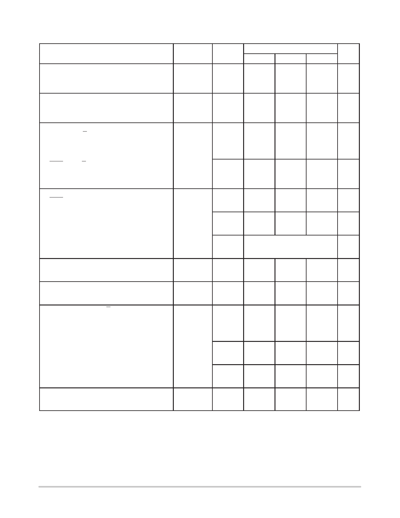
ÎÎÎÎÎÎÎÎÎÎÎÎÎÎÎÎÎÎÎÎÎÎÎÎÎÎÎÎÎÎÎÎÎ SWITCHING CHARACTERISTICS (6.) (CL = 50 pF, TA = 25_C)
ÎÎÎÎÎÎÎÎÎÎÎÎÎÎÎÎÎÎÎÎÎÎÎÎÎÎÎÎÎÎÎÎÎ VDD
All Types
Characteristic
Symbol
Vdc
Min
Typ (7.)
Max
Unit
Output Rise Time
tTLH = (1.35 ns/pF) CL + 33 ns
tTLH = (0.60 ns/pF) CL + 20 ns
tTLH = (0.40 ns/pF) CL + 20 ns
Output Fall Time
tTHL = (1.35 ns/pF) CL + 33 ns
tTHL = (0.60 ns/pF) CL + 20 ns
tTHL = (0.40 ns/pF) CL + 20 ns
Propagation Delay Time
A or B to Q or Q
tPLH, tPHL = (0.90 ns/pF) CL + 255 ns
tPLH, tPHL = (0.36 ns/pF) CL + 132 ns
tPLH, tPHL = (0.26 ns/pF) CL + 87 ns
tTLH
ns
5.0
—
100
200
10
—
50
100
15
—
40
80
tTHL
ns
5.0
—
100
200
10
—
50
100
15
—
40
80
tPLH,
ns
tPHL
5.0
—
300
600
10
—
150
300
15
—
100
220
Reset to Q or Q
tPLH, tPHL = (0.90 ns/pF) CL + 205 ns
tPLH, tPHL = (0.36 ns/pF) CL + 107 ns
tPLH, tPHL = (0.26 ns/pF) CL + 82 ns
Input Rise and Fall Times
Reset
ns
5.0
—
250
500
10
—
125
250
15
—
95
190
tr, tf
5
—
—
15
µs
10
—
—
5
15
—
—
4
B Input
5
—
300
1.0
ms
10
—
1.2
0.1
15
—
0.4
0.05
A Input
5
—
10
No Limit
15
Input Pulse Width
A, B, or Reset
tWH,
5.0
170
85
—
ns
tWL
10
90
45
—
15
80
40
—
Retrigger Time
trr
5.0
0
—
—
ns
10
0
—
—
15
0
—
—
Output Pulse Width — Q or Q
Refer to Figures 8 and 9
CX = 0.002 µF, RX = 100 kΩ
T
µs
5.0
198
210
230
10
200
212
232
15
202
214
234
CX = 0.1 µF, RX = 100 kΩ
5.0
9.3
9.86
10.5
ms
10
9.4
10
10.6
15
9.5
10.14
10.7
CX = 10 µF, RX = 100 kΩ
5.0
0.91
0.965
1.03
s
10
0.92
0.98
1.04
15
0.93
0.99
1.06
Pulse Width Match between circuits in
the same package.
CX = 0.1 µF, RX = 100 kΩ
100
5.0
[(T1 – T2)/T1]
10
15
—
± 1.0
± 5.0
%
—
± 1.0
± 5.0
—
± 1.0
± 5.0
6. The formulas given are for the typical characteristics only at 25_C.
7. Data labelled “Typ” is not to be used for design purposes but is intended as an indication of the IC’s potential performance.
http://onsemi.com
4
Share Link: 