MC14538BFR1 Просмотр технического описания (PDF) - ON Semiconductor
Номер в каталоге
Компоненты Описание
производитель
MC14538BFR1 Datasheet PDF : 12 Pages
| |||
MC14538B
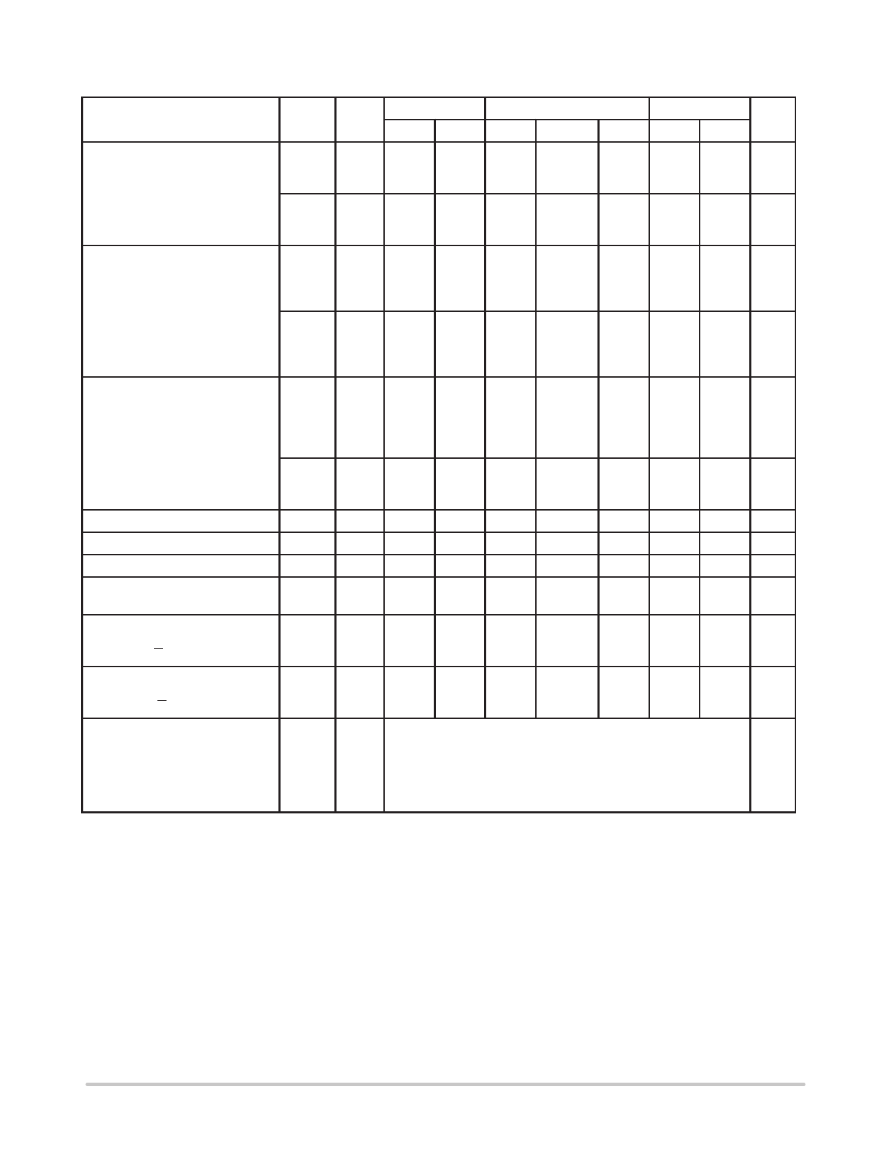
ÎÎÎÎÎÎÎÎÎÎÎÎÎÎÎÎÎÎÎÎÎÎÎÎÎÎÎÎÎÎÎÎÎ ELECTRICAL CHARACTERISTICS (Voltages Referenced to VSS)
ÎÎÎÎÎÎÎÎÎÎÎÎÎÎÎÎÎÎÎÎÎÎÎÎÎÎÎÎÎÎÎÎÎ VDD
– 55_C
25_C
125_C
Characteristic
Symbol Vdc
Min
Max
Min Typ (4.) Max
Min
Max Unit
Output Voltage
Vin = VDD or 0
“0” Level VOL
5.0
10
15
—
0.05
—
—
0.05
—
—
0.05
—
0
0.05
—
0.05 Vdc
0
0.05
—
0.05
0
0.05
—
0.05
Vin = 0 or VDD
“1” Level VOH
5.0
4.95
—
4.95
5.0
10
9.95
—
9.95
10
15
14.95
—
14.95
15
—
4.95
—
Vdc
—
9.95
—
—
14.95
—
Input Voltage
“0” Level VIL
(VO = 4.5 or 0.5 Vdc)
(VO = 9.0 or 1.0 Vdc)
(VO = 13.5 or 1.5 Vdc)
“1” Level VIH
(VO = 0.5 or 4.5 Vdc)
(VO = 1.0 or 9.0 Vdc)
(VO = 1.5 or 13.5 Vdc)
Output Drive Current
(VOH = 2.5 Vdc)
(VOH = 4.6 Vdc)
(VOH = 9.5 Vdc)
(VOH = 13.5 Vdc)
IOH
Source
5.0
—
1.5
—
2.25
10
—
3.0
—
4.50
15
—
4.0
—
6.75
5.0
3.5
—
3.5
2.75
10
7.0
—
7.0
5.50
15
11
—
11
8.25
5.0 – 3.0
—
– 2.4
– 4.2
5.0 – 0.64 — – 0.51 – 0.88
10
– 1.6
—
– 1.3 – 2.25
15
– 4.2
—
– 3.4
– 8.8
Vdc
1.5
—
1.5
3.0
—
3.0
4.0
—
4.0
Vdc
—
3.5
—
—
7.0
—
—
11
—
mAdc
—
– 1.7
—
— – 0.36 —
—
– 0.9
—
—
– 2.4
—
(VOL = 0.4 Vdc)
(VOL = 0.5 Vdc)
(VOL = 1.5 Vdc)
Sink IOL
Input Current, Pin 2 or 14
Iin
Input Current, Other Inputs
Iin
Input Capacitance, Pin 2 or 14
Cin
Input Capacitance, Other Inputs
Cin
(Vin = 0)
Quiescent Current
IDD
(Per Package)
Q = Low, Q = High
5.0
0.64
—
0.51
0.88
10
1.6
—
1.3
2.25
15
4.2
—
3.4
8.8
—
0.36
— mAdc
—
0.9
—
—
2.4
—
15
—
± 0.05
— ± 0.00001 ± 0.05
—
± 0.5 µAdc
15
—
± 0.1
— ± 0.00001 ± 0.1
—
± 1.0 µAdc
—
—
—
—
25
—
—
—
pF
—
—
—
—
5.0
7.5
—
—
pF
5.0
—
5.0
—
0.005
5.0
—
150 µAdc
10
—
10
—
0.010
10
—
300
15
—
20
—
0.015
20
—
600
Quiescent Current, Active State
(Both) (Per Package)
Q = High, Q = Low
IDD
5.0
—
10
—
15
—
2.0
—
2.0
—
2.0
—
0.04
0.20
—
2.0 mAdc
0.08
0.45
—
2.0
0.13
0.70
—
2.0
Total Supply Current at an external
IT
5.0
load capacitance (CL) and at
10
external timing network (RX, CX) (5.)
IT = (3.5 x 10⁻²) RXCXf + 4CXf + 1 x 10⁻⁵ CLf
IT = (8.0 x 10⁻²) RXCXf + 9CXf + 2 x 10⁻⁵ CLf
IT = (1.25 x 10⁻¹) RXCXf + 12CXf + 3 x 10⁻⁵ CLf
where: IT in µA (one monostable switching only),
where: CX in µF, CL in pF, RX in k ohms, and
where: f in Hz is the input frequency.
µAdc
4. Data labelled “Typ” is not to be used for design purposes but is intended as an indication of the IC’s potential performance.
5. The formulas given are for the typical characteristics only at 25_C.
http://onsemi.com
3
Share Link: 