KSC5502D(2001) Просмотр технического описания (PDF) - Fairchild Semiconductor
Номер в каталоге
Компоненты Описание
производитель
KSC5502D Datasheet PDF : 11 Pages
| |||
KSC5502D/KSC5502DT
High Voltage Power Switch Switching
Application
• Wide Safe Operating Area
• Built-in Free-Wheeling Diode
• Suitable for Electronic Ballast Application
• Small Variance in Storage Time
• Two Package Choices : D-PAK or TO-220
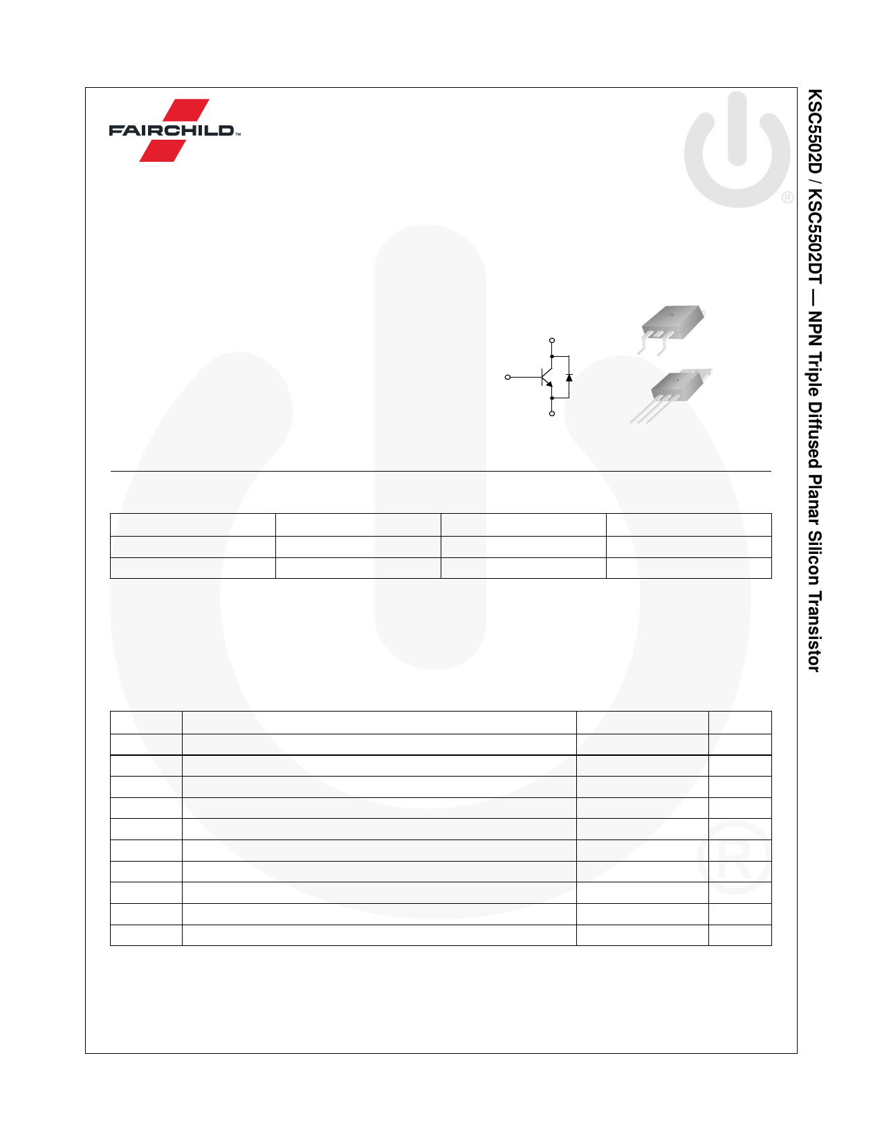
Equivalent Circuit
C
B
D-PAK
1
TO-220
E
1
1.Base 2.Collector 3.Emitter
NPN Triple Diffused Planar Silicon Transistor
Absolute Maximum Ratings TC=25°C unless otherwise noted
Symbol
Parameter
VCBO
Collector-Base Voltage
V CEO
Collector-Emitter Voltage
VEBO
Emitter-Base Voltage
IC
Collector Current (DC)
ICP
*Collector Current (Pulse)
IB
Base Current (DC)
IBP
*Base Current (Pulse)
PC
Collector Dissipation (TC=25°C)
TJ
Junction Temperature
TSTG
Storage Temperature
EAS
Avalanche Energy(Tj=25°C)
* Pulse Test : Pulse Width = 5ms, Duty Cycle ≤ 10%
Value
1200
600
12
2
4
1
2
50
150
- 65 ~ 150
2.5
Units
V
V
V
A
A
A
A
W
°C
°C
mJ
Thermal Characteristics TC=25°C unless otherwise noted
Symbol
Characteristics
Rθjc
Thermal Resistance
Junction to Case
Rθja
Junction to Ambient
TL
Maximun Lead Temperature for Soldering Purpose
: 1/8” from Case for 5 seconds
Rating
2.5
62.5
270
Unit
°C/W
°C
©2001 Fairchild Semiconductor Corporation
Rev. A2, August 2001
Share Link: 